SNOS018H August 1999 – December 2014 LMV331-N , LMV339-N , LMV393-N
PRODUCTION DATA.
- 1 Features
- 2 Applications
- 3 Description
- 4 Revision History
- 5 Pin Configuration and Functions
- 6 Specifications
- 7 Detailed Description
- 8 Application and Implementation
- 9 Power Supply Recommendations
- 10Layout
- 11Device and Documentation Support
- 12Mechanical, Packaging, and Orderable Information
Package Options
Mechanical Data (Package|Pins)
Thermal pad, mechanical data (Package|Pins)
Orderable Information
7 Detailed Description
7.1 Overview
The LMV331-N/393-N/339-N comparators features a supply voltage range of 2.7 V to 5 V with a low supply current of 55 μA/channel with propagation delays as low as 200ns. They are avaialble in small, space-saving packages, which makes these comparators versatile for use in a wide range of applications, from portable to industrial. The open collector output configuration allows the device to be used in wired-OR configurations, such as a window comparators.
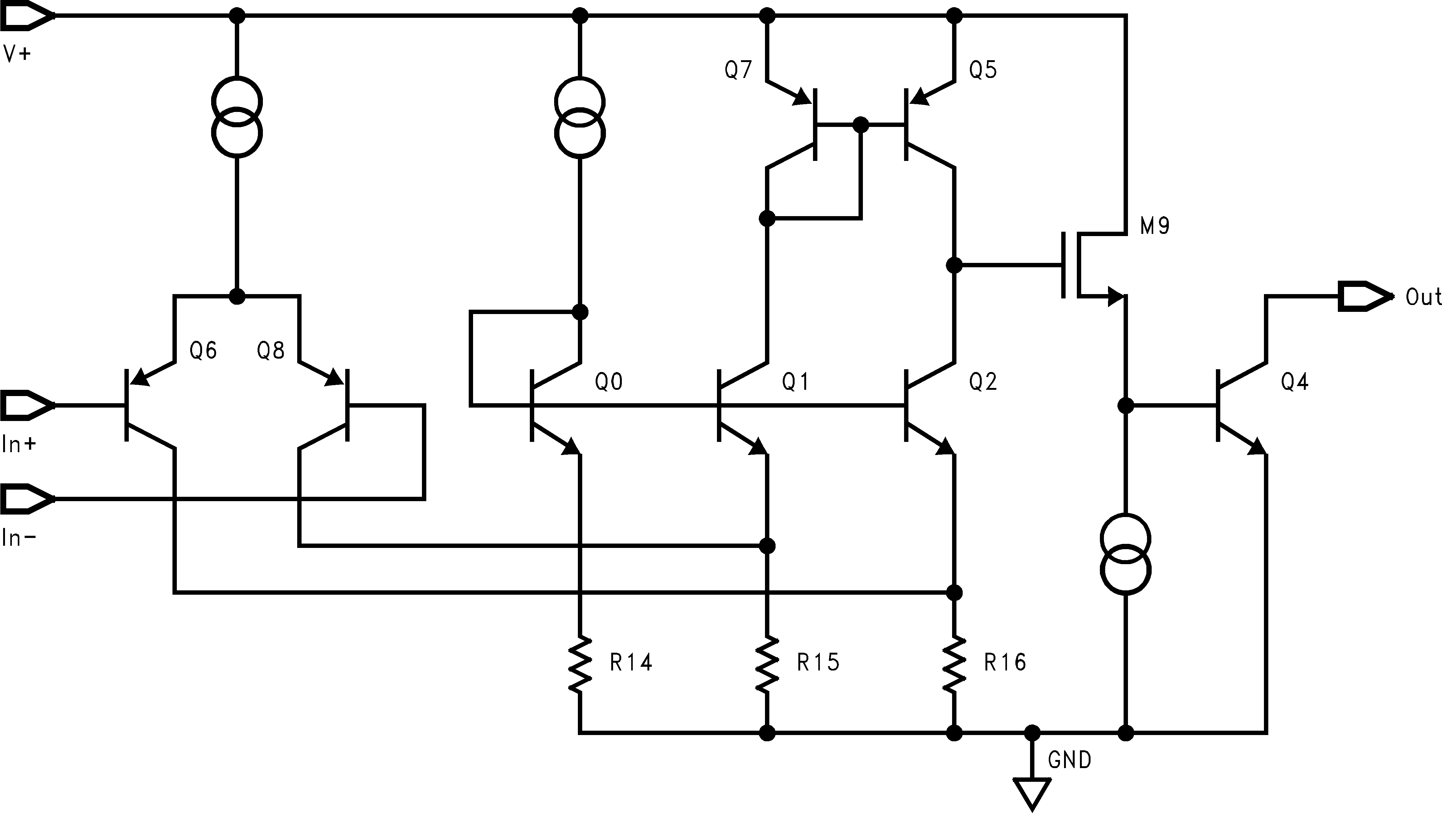
7.2 Functional Block Diagram
7.3 Feature Description
7.3.1 Open Collector Output
The output of the LMV331-N/393-N/339-N series is the uncommitted collector of a grounded-emitter NPN output transistor, which requires a pull-up resistor to a positive supply voltage for the output to switch properly. Many collectors can be tied together to provide an output OR’ing function. An output pull-up resistor can be connected to any available power supply voltage within the permitted V+ supply voltage range. The output pull-up resistor should be chosen high enough so as to avoid excessive power dissipation yet low enough to supply enough drive to switch whatever load circuitry is used on the comparator output. On the LMV331-N/393-N/339-N the pull-up resistor should range between 1 k to 10 kΩ.
7.3.2 Ground Sensing Input
The LMV331-N/393-N/339-N has a typical input common mode voltage range of −0.1V below the ground to 0.8V below Vcc.
7.4 Device Functional Modes
A basic comparator circuit is used for converting analog signals to a digital output.
The output is HIGH when the voltage on the non-inverting (+IN) input is greater than the inverting (-IN) input.
The output is LOW when the voltage on the non-inverting (+IN) input is less than the inverting (-IN) input.
The inverting input (-IN) is also commonly referred to as the "reference" or "VREF" input.