SNOSAG6G September 2005 – October 2015 LMV791 , LMV792
PRODUCTION DATA.
- 1 Features
- 2 Applications
- 3 Description
- 4 Revision History
- 5 Pin Configuration and Functions
- 6 Specifications
- 7 Detailed Description
- 8 Application and Implementation
- 9 Power Supply Recommendations
- 10Layout
- 11Device and Documentation Support
- 12Mechanical, Packaging, and Orderable Information
Package Options
Mechanical Data (Package|Pins)
- DDC|6
Thermal pad, mechanical data (Package|Pins)
Orderable Information
8 Application and Implementation
NOTE
Information in the following applications sections is not part of the TI component specification, and TI does not warrant its accuracy or completeness. TI’s customers are responsible for determining suitability of components for their purposes. Customers should validate and test their design implementation to confirm system functionality.
8.1 Application Information
The LMV791 and LMV792 family of amplifiers is specified for operation from 1.8 V to 5.5 V. Parameters that can exhibit significant variance with regard to operating voltage or temperature are presented in the Typical Characteristics section.
8.2 Typical Applications
These application examples highlight a few of the circuits where the LMV791 and LMV792 may be used.
8.2.1 Transimpedance Amplifier
CMOS input operational amplifiers are often used in transimpedance applications as they have an extremely high input impedance. A transimpedance amplifier converts a small input current into a voltage. This current is usually generated by a photodiode. The transimpedance gain, measured as the ratio of the output voltage to the input current, is expected to be large and wide-band. Because the circuit deals with currents in the range of a few nA, low-noise performance is essential. The LMV79x are CMOS input operational amplifiers providing wide bandwidth and low noise performance, and are hence ideal for transimpedance applications.
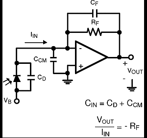 Figure 50. Photodiode Transimpedance Amplifier
8.2.1.1 Design Requirements
Usually, a transimpedance amplifier is designed on the basis of the current source driving the input. A photodiode is a very common capacitive current source, which requires transimpedance gain for transforming its miniscule current into easily-detectable voltages. The photodiode and gain of the amplifier are selected with respect to the speed and accuracy required of the circuit. A faster circuit would require a photodiode with lesser capacitance and a faster amplifier. A more sensitive circuit would require a sensitive photodiode and a high gain. A typical transimpedance amplifier is shown in Figure 50. The output voltage of the amplifier is given by the equation VOUT = −IINRF. Because the output swing of the amplifier is limited, RF should be selected such that all possible values of IIN can be detected.
8.2.1.2 Detailed Design Procedure
The LMV79x have a large gain-bandwidth product (17 MHz), which enables high gains at wide bandwidths. A rail-to-rail output swing at 5.5-V supply allows detection and amplification of a wide range of input currents. A CMOS input stage with negligible input current noise and low input voltage noise allows the LMV79x to provide high-fidelity amplification for wide bandwidths. These properties make the LMV79x ideal for systems requiring wide-band transimpedance amplification.
As mentioned earlier, the following parameters are used to design a transimpedance amplifier: the amplifier gain-bandwidth product, A0; the amplifier input capacitance, CCM; the photodiode capacitance, CD; the transimpedance gain required, RF; and the amplifier output swing. Once a feasible RF is selected using the amplifier output swing, these numbers can be used to design an amplifier with the desired transimpedance gain and a maximally flat frequency response.
An essential component for obtaining a maximally flat response is the feedback capacitor, CF. The capacitance seen at the input of the amplifier, CIN, combined with the feedback capacitor, RF, generate a phase lag which causes gain-peaking and can destabilize the circuit. CIN is usually just the sum of CD and CCM. The feedback capacitor CF creates a pole, fP in the noise gain of the circuit, which neutralizes the zero in the noise gain, fZ, created by the combination of RF and CIN. If properly positioned, the noise gain pole created by CF can ensure that the slope of the gain remains at 20 dB/decade till the unity gain frequency of the amplifier is reached, thus ensuring stability. As shown in Figure 51, fP is positioned such that it coincides with the point where the noise gain intersects the open-loop gain of the operational amplifier. In this case, fP is also the overall 3-dB frequency of the transimpedance amplifier. The value of CF needed to make it so is given by Equation 3. A larger value of CF causes excessive reduction of bandwidth, while a smaller value fails to prevent gain peaking and instability.
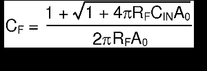
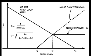 Figure 51. CF Selection for Stability
Calculating CF from Equation 3 can sometimes return unreasonably small values (<1 pF), especially for high-speed applications. In these cases, its often more practical to use the circuit shown in Figure 52 in order to allow more reasonable values. In this circuit, the capacitance CF′ is (1+ RB/RA) time the effective feedback capacitance, CF. A larger capacitor can now be used in this circuit to obtain a smaller effective capacitance.
For example, if a CF of 0.5 pF is needed, while only a 5-pF capacitor is available, RB and RA can be selected such that RB/RA = 9. This would convert a CF′ of 5 pF into a CF of 0.5 pF. This relationship holds as long as RA < RF.
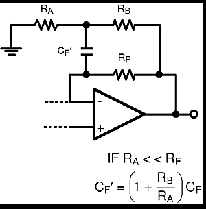 Figure 52. Obtaining Small CF from large CF′
8.2.2 Application Curves
The LMV791 was used to design a number of amplifiers with varying transimpedance gains and source capacitances. The gains, bandwidths and feedback capacitances of the circuits created are summarized in Table 1. The frequency responses are presented in Figure 53 and Figure 54. The feedback capacitances are slightly different from the formula in Equation 3, because the parasitic capacitance of the board and the feedback resistor RF had to be accounted for.
Table 1. Frequency Response Results
| Transimpedance, ATI | CIN | CF | 3-dB Frequency |
|---|---|---|---|
| 470000 | 50 pF | 1.5 pF | 350 kHz |
| 470000 | 100 pF | 2.0 pF | 250 kHz |
| 470000 | 200 pF | 3.0 pF | 150 kHz |
| 47000 | 50 pF | 4.5 pF | 1.5 MHz |
| 47000 | 100 pF | 6.0 pF | 1 MHz |
| 47000 | 200 pF | 9.0 pF | 700 kHz |
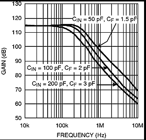 Figure 53. Frequency Response for ATI = 470000
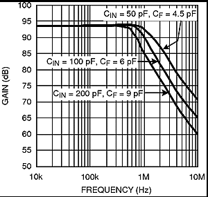 Figure 54. Frequency Response for ATI = 47000
8.2.3 High-Gain, Wideband Transimpedance Amplifier Using the LMV792
The LMV792, dual, low-noise, wide-bandwidth, CMOS input operational amplifier IC can be used for compact, robust and integrated solutions for sensing and amplifying wide-band signals obtained from sensitive photodiodes. One of the two operational amplifiers available can be used to obtain transimpedance gain while the other can be used for amplifying the output voltage to further enhance the transimpedance gain. The wide bandwidth of the operational amplifiers (17 MHz) ensures that they are capable of providing high gain for a wide range of frequencies. The low input referred noise (5.8 nV/√Hz) allows the amplifier to deliver an output with a high SNR (signal to noise ratio). The small VSSOP-10 footprint saves space on printed-circuit-boards and allows ease of design in portable products.
The circuit shown in Figure 55, has the first operational amplifier acting as a transimpedance amplifier with a gain of 47000, while the second stage provides a voltage gain of 10. This provides a total transimpedance gain of 470000 with a −3-dB bandwidth of about 1.5 MHz, for a total input capacitance of 50 pF. The frequency response for the circuit is shown in Figure 56
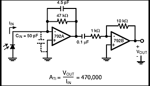 Figure 55. 1.5-MHz Transimpedance Amplifier, With ATI = 470000
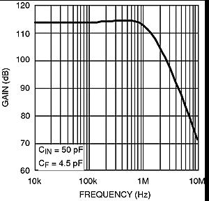 Figure 56. 1.5-MHz Transimpedance Amplifier Frequency Response
8.2.4 Audio Preamplifier With Bandpass Filtering
With low input referred voltage noise, low supply voltage and low supply current, and a low harmonic distortion, the LMV791 family is ideal for audio applications. Its wide unity gain bandwidth allows it to provide large gain for a wide range of frequencies and it can be used to design a preamplifier to drive a load of as low as 600 Ω with less than 0.01% distortion. Two amplifier circuits are shown in Figure 57 and Figure 58. Figure 57 is an inverting amplifier, with a 10-kΩ feedback resistor, R2, and a 1-kΩ input resistor, R1, and hence provides a gain of −10. Figure 58 is a noninverting amplifier, using the same values of R1and R2, and provides a gain of 11. In either of these circuits, the coupling capacitor CC1 decides the lower frequency at which the circuit starts providing gain, while the feedback capacitor CF decides the frequency at which the gain starts dropping off. Figure 59 shows the frequency response of the inverting amplifier with different values of CF.
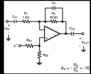 Figure 57. Inverting Audio Preamplifier
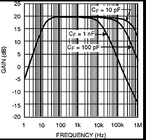 Figure 59. Frequency Response of the Inverting Audio Preamplifier
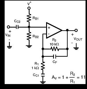 Figure 58. Noninverting Audio Preamplifier
8.2.5 Sensor Interfaces
The low input bias current and low input referred noise of the LMV791 and LMV792 make them ideal for sensor interfaces. These circuits are required to sense voltages of the order of a few μV, and currents amounting to less than a nA, and hence the operational amplifier needs to have low voltage noise and low input bias current. Typical applications include infrared (IR) thermometry, thermocouple amplifiers and pH electrode buffers. Figure 60 is an example of a typical circuit used for measuring IR radiation intensity, often used for estimating the temperature of an object from a distance. The IR sensor generates a voltage proportional to I, which is the intensity of the IR radiation falling on it. As shown in Figure 60, K is the constant of proportionality relating the voltage across the IR sensor (VIN) to the radiation intensity, I. The resistances RA and RB are selected to provide a high gain to amplify this voltage, while CF is added to filter out the high-frequency noise.
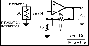 Figure 60. IR Radiation Sensor