SNOSAG6G September 2005 – October 2015 LMV791 , LMV792
PRODUCTION DATA.
- 1 Features
- 2 Applications
- 3 Description
- 4 Revision History
- 5 Pin Configuration and Functions
- 6 Specifications
- 7 Detailed Description
- 8 Application and Implementation
- 9 Power Supply Recommendations
- 10Layout
- 11Device and Documentation Support
- 12Mechanical, Packaging, and Orderable Information
Package Options
Mechanical Data (Package|Pins)
- DDC|6
Thermal pad, mechanical data (Package|Pins)
Orderable Information
10 Layout
10.1 Layout Guidelines
Connect low-ESR, 0.1-μF ceramic bypass capacitors between each supply pin and ground, placed as close to the device as possible. A single bypass capacitor from V+ to ground is applicable for single-supply applications.
Noise can propagate into analog circuitry through the power pins of the circuit as a whole and operational amplifier itself. Bypass capacitors are used to reduce the coupled noise by providing low-impedance power sources local to the analog circuitry.
Separate grounding for analog and digital portions of circuitry is one of the simplest and most-effective methods of noise suppression. One or more layers on multilayer PCBs are usually devoted to ground planes. A ground plane helps distribute heat and reduces EMI noise pickup. Make sure to physically separate digital and analog grounds, paying attention to the flow of the ground current.
The ground pin should be connected to the PCB ground plane at the pin of the device.
The feedback components should be placed as close to the device as possible minimizing strays.
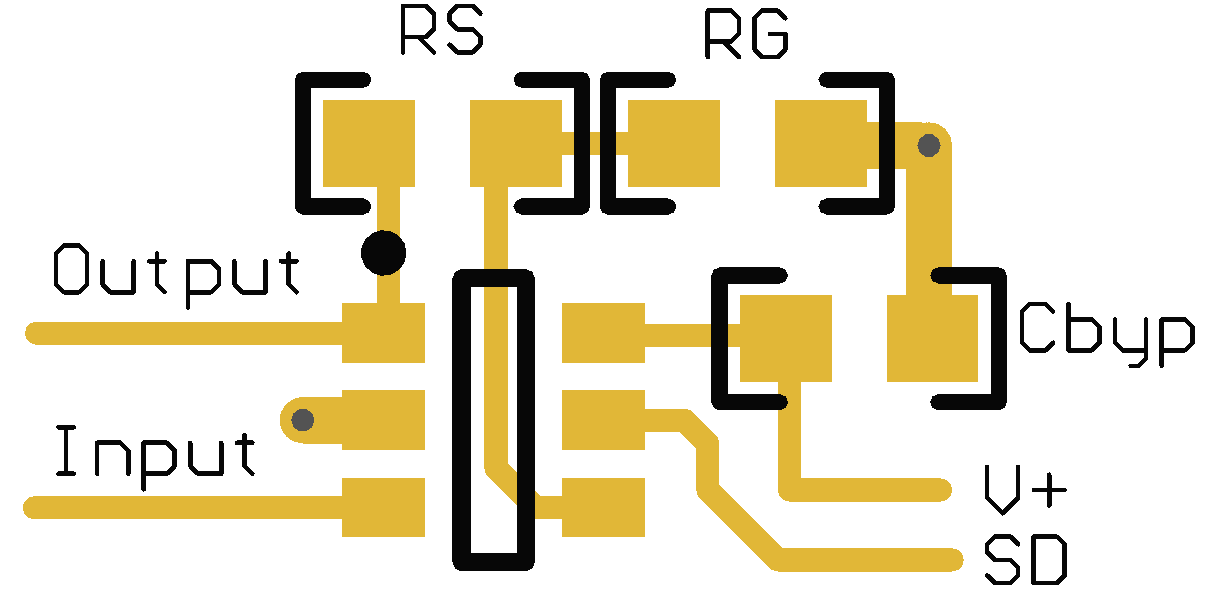
10.2 Layout Example
 Figure 61. Typical SOT Layout