SNAS624B March 2014 – May 2015 LMX2492 , LMX2492-Q1
PRODUCTION DATA.
- 1 Features
- 2 Applications
- 3 Description
- 4 Simplified Schematic
- 5 Revision History
- 6 Pin Configuration and Functions
- 7 Specifications
-
8 Detailed Description
- 8.1 Overview
- 8.2 Functional Block Diagram
- 8.3
Feature Description
- 8.3.1 OSCin Input
- 8.3.2 OSCin Doubler
- 8.3.3 R Divider
- 8.3.4 PLL N Divider
- 8.3.5 Fractional Circuitry
- 8.3.6 PLL Phase Detector and Charge Pump
- 8.3.7 External Loop Filter
- 8.3.8 Fastlock and Cycle Slip Reduction
- 8.3.9 Lock Detect and Charge Pump Voltage Monitor
- 8.3.10 FSK/PSK Modulation
- 8.3.11 Ramping Functions
- 8.3.12 Power on Reset (POR)
- 8.4 Device Functional Modes
- 8.5 Programming
- 8.6 Register Map
- 8.7 Register Field Descriptions
- 8.8 Lock Detect and Charge Pump Monitoring
- 8.9 TRIG1,TRIG2,MOD, and MUXout Pins
- 8.10 Ramping Functions
- 8.11 Individual Ramp Controls
- 9 Applications and Implementation
- 10Power Supply Recommendations
- 11Layout
- 12Device and Documentation Support
- 13Mechanical, Packaging, and Orderable Information
Package Options
Mechanical Data (Package|Pins)
- RTW|24
Thermal pad, mechanical data (Package|Pins)
- RTW|24
Orderable Information
7 Specifications
7.1 Absolute Maximum Ratings
over operating free-air temperature range (unless otherwise noted) (1)| MIN | MAX | UNIT | ||
|---|---|---|---|---|
| Vcp | Supply voltage for charge pump | Vcc | 5.5 | V |
| CPout | Charge pump output pin | -0.3 | Vcp | V |
| Vcc | All Vcc pins | -0.3 | 3.6 | V |
| Others | All other I/O pins | -0.3 | Vcc + 0.3 | V |
| TSolder | Lead temperature (solder 4 seconds) | 260 | °C | |
| TJunction | Junction temperature | 150 | °C |
(1) Stresses beyond those listed under Absolute Maximum Ratings may cause permanent damage to the device. These are stress ratings only, which do not imply functional operation of the device at these or any other conditions beyond those indicated under Recommended Operating Conditions. Exposure to absolute-maximum-rated conditions for extended periods may affect device reliability.
7.2 Storage Conditions
applicable before the DMD is installed in the final product| MIN | MAX | UNIT | ||
|---|---|---|---|---|
| Tstg | DMD storage temperature | -65 | 150 | °C |
| MSL | Moisture sensitivity level | 3 | n/a | |
7.3 ESD Ratings
| VALUE | UNIT | |||
|---|---|---|---|---|
| V(ESD) | Electrostatic discharge | Human-body model (HBM), per ANSI/ESDA/JEDEC JS-001(1) | ±2500 | V |
| Charged-device model (CDM), per JEDEC specification JESD22-C101(2) | ±1500 | |||
(1) JEDEC document JEP155 states that 500-V HBM allows safe manufacturing with a standard ESD control process.
(2) JEDEC document JEP157 states that 250-V CDM allows safe manufacturing with a standard ESD control process.
7.4 Recommended Operating Conditions
over operating free-air temperature range (unless otherwise noted)7.5 Thermal Information
| THERMAL METRIC(1) | LMX2492 RTW (WQFN ) 24 PINS |
UNIT | |
|---|---|---|---|
| RθJA | Junction-to-ambient thermal resistance | 39.4 | °C/W |
| RθJC | Junction-to-case thermal resistance | 7.1 | |
| ψJB | Junction-to-board characterization parameter | 20 |
(1) For more information about traditional and new thermal metrics, see the IC Package Thermal Metrics application report, SPRA953.
7.6 Electrical Characteristics
(3.15 V ≤ Vcc ≤ 3.45 V. Vcc ≤Vcp ≤5.25 V. Typical values are at Vcc = Vcp = 3.3 V, 25 °C.-40°C ≤ TA ≤ 85 °C for the LMX2492 and -40°C ≤ TA ≤ 125 °C for the LMX2492-Q1 ; except as specified.)
| PARAMETER | CONDITIONS | MIN | TYP | MAX | UNIT | ||
|---|---|---|---|---|---|---|---|
| Icc | Current Consumption | All Vcc Pins | Fpd = 10 MHz | 45 | mA | ||
| Fpd = 100 MHz | 50 | ||||||
| Fpd = 200 MHz | 55 | ||||||
| Vcp Pin | Kpd = 0.1 mA | 2 | |||||
| Kpd = 1.6 mA | 10 | ||||||
| Kpd = 3.1 mA | 19 | ||||||
| IccPD | Current | POWERDOWN | 3 | ||||
| fOSCin | Frequency for OSCin terminal | OSC_DIFFR=0, Doubler Disabled | 10 | 600 | MHz | ||
| OSC_DIFFR=0, Doubler Enabled | 10 | 300 | |||||
| OSC_DIFFR=1, Doubler Disabled | 10 | 1200 | |||||
| OSC_DIFFR=1, Doubler Enabled | 10 | 600 | |||||
| vOSCin | Voltage for OSCin Pin(1) | LMX2492-Q1 Version Only Single Ended XO 30 MHz ≤ fOSCin ≤ 100 MHz |
0.24 | Vcc-0.5 | Vpp | ||
| All Other Cases | 0.5 | Vcc-0.5 | |||||
| fFin | Frequency for FinPin(4) | 500 | 14000 | MHz | |||
| pFin | Power for Fin Pin | Single-Ended Operation | -5 | 5 | dBm | ||
| fPD | Phase Detector Frequency | 200 | MHz | ||||
| PN1Hz | PLL Figure of Merit(2) | -227 | dBc/Hz | ||||
| PN10kHz | Normalized PLL 1/f Noise(2) | Normalized to 10 kHz offset for a 1 GHz carrier. | -120 | dBc/Hz | |||
| ICPoutTRI | Charge Pump Leakage Tri-state Leakage | 10 | nA | ||||
| ICPoutMM | Charge Pump Mismatch(3) | VCPout = Vcp / 2 | 5 % | ||||
| ICPout | Charge Pump Current | VCPout = Vcp / 2 | CPG=1X | 0.1 | mA | ||
| … | |||||||
| CPG=31X | 3.1 | ||||||
| LOGIC OUTPUT TERMINALS (MUXout,TRIG1,TRIG2,MOD) | |||||||
| VOH | Output High Voltage | 0.8 x Vcc | Vcc | V | |||
| VOL | Output Low Voltage | 0 | 0.2 x Vcc | V | |||
| LOGIC INPUT TERMINALS (CE,CLK,DATA,LE,MUXout,TRIG1,TRIG2,MOD) | |||||||
| VIH | Input High Voltage | 1.4 | Vcc | V | |||
| VIL | Input Low Voltage | 0 | 0.6 | V | |||
| IIH | Input Leakage | -5 | 1 | 5 | uA | ||
| TCELOW | Chip enable Low Time | 5 | us | ||||
| TCEHIGH | Chip enable High Time | 5 | us | ||||
(1) For optimal phase noise performance, a slew rate of at least 3 V/ns is recommended
(2) PLL Noise Metrics are measured with a clean OSCin signal with a high slew rate using a wide loop bandwidth. The noise metrics model the PLL noise for an infinite loop bandwidth as:
PLL_Total = 10×log( 10PLL_Flat/10 + 10PLL_Flicker(Offset)/10)
PLL_Flat = PN1Hz + 20×log(N) + 10×log(Fpd/1Hz)
PLL_Flicker = PN10kHz - 10×log(Offset/10kHz) + 20×log(Fvco/1GHz)
PLL_Total = 10×log( 10PLL_Flat/10 + 10PLL_Flicker(Offset)/10)
PLL_Flat = PN1Hz + 20×log(N) + 10×log(Fpd/1Hz)
PLL_Flicker = PN10kHz - 10×log(Offset/10kHz) + 20×log(Fvco/1GHz)
(3) Charge pump mismatch varies as a function of charge pump voltage. Consult typical performance characteristics to see this variation.
(4) Tested to 13.5 GHz, Guaranteed to 14 GHz by characterization
7.7 Timing Requirements, Programming Interface (CLK, DATA, LE)
There are several other considerations for programming:
- The DATA is clocked into a shift register on each rising edge of the CLK signal. On the rising edge of the LE signal, the data is sent from the shift register to an actual counter.
- If no LE signal is given after the last data bit and the clock is kept toggling, then these bits will be read into the next lower register. This eliminates the need to send the address each time.
- A slew rate of at least 30 V/us is recommended for the CLK, DATA, and LE signals
- Timing specifications also apply to readback. Readback can be done through the MUXout, TRIG1, TRIG2, or MOD terminals.
7.8 Typical Characteristics

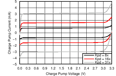
For a charge pump supply of 3.3 V, optimal performance is for a typical charge pump output voltage between 0.5 and 2.8 volts.
Figure 2. Charge Pump Current for Vcp = 3.3 V

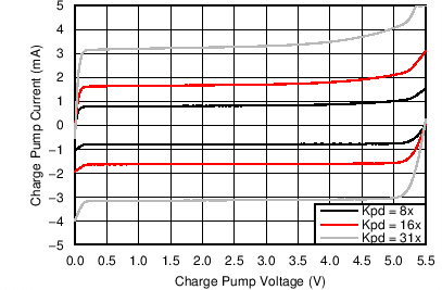
For a charge pump supply voltage of 5 volts or higher, optimal performance is typically for a charge pump output voltage between 0.5 and 4.5 volts.
Figure 3. Charge Pump Current for Vcp = 5.5 V

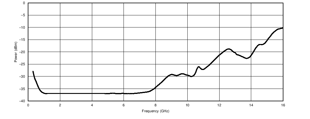
Typical value of lowest power level as a function of frequency. Design to electrical specifications for input sensitivity, not typical performance graphs.
Figure 4. Fin Input Sensitivity

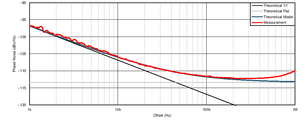
This plot is for a phase detector of 100 MHz, 2 MHz loop bandwidth, and VCO at 9600 MHz. However, the plot shown is the divide by 2 port at 4800 MHz. The input was a 100 MHz Wenzel Oscillator. The model shows this phase noise has a figure of merit of -227 dBc/Hz and a normalized 1/f noise of -120.5 dBc/Hz. The charge pump supply was 5 V and the charge pump output voltage was 1.34 V.
Figure 5. LMX2492/92-Q1 Phase Noise for Fpd =100 MHz, Fvco = 9600 MHz/2
