SNVSB57A October   2018  – May 2019 LMZM33604

PRODUCTION DATA.  

  1. Features
  2. Applications
    1.     Simplified Schematic
  3. Description
    1.     Minimum Solution Size
    2.     Typical Efficiency (Auto Mode)
  4. Revision History
  5. Pin Configuration and Functions
    1.     Pin Functions
  6. Specifications
    1. 6.1 Absolute Maximum Ratings
    2. 6.2 ESD Ratings
    3. 6.3 Recommended Operating Conditions
    4. 6.4 Thermal Information
    5. 6.5 Electrical Characteristics
    6. 6.6 Switching Characteristics
    7. 6.7 Typical Characteristics (VIN = 12 V)
    8. 6.8 Typical Characteristics (VIN = 24 V)
    9. 6.9 Typical Characteristics (VIN = 36 V)
  7. Detailed Description
    1. 7.1 Overview
    2. 7.2 Functional Block Diagram
    3. 7.3 Feature Description
      1. 7.3.1  Adjusting the Output Voltage
      2. 7.3.2  Input Capacitor Selection
      3. 7.3.3  Output Capacitor Selection
      4. 7.3.4  Transient Response
      5. 7.3.5  Feed-Forward Capacitor
      6. 7.3.6  Switching Frequency (RT)
      7. 7.3.7  Synchronization (SYNC/MODE)
      8. 7.3.8  Output Enable (EN)
      9. 7.3.9  Programmable System UVLO (EN)
      10. 7.3.10 Internal LDO and BIAS_SEL
      11. 7.3.11 Power Good (PGOOD) and Power Good Pullup (PGOOD_PU)
      12. 7.3.12 Mode Select (Auto or FPWM)
      13. 7.3.13 Soft Start and Voltage Tracking
      14. 7.3.14 Voltage Dropout
      15. 7.3.15 Overcurrent Protection (OCP)
      16. 7.3.16 Thermal Shutdown
    4. 7.4 Device Functional Modes
      1. 7.4.1 Active Mode
      2. 7.4.2 Auto Mode
      3. 7.4.3 FPWM Mode
      4. 7.4.4 Shutdown Mode
  8. Application and Implementation
    1. 8.1 Application Information
    2. 8.2 Typical Application
      1. 8.2.1 Design Requirements
      2. 8.2.2 Detailed Design Procedure
        1. 8.2.2.1 Output Voltage Setpoint
        2. 8.2.2.2 Setting the Switching Frequency
        3. 8.2.2.3 Input Capacitors
        4. 8.2.2.4 Output Capacitor Selection
        5. 8.2.2.5 Feed-Forward Capacitor (CFF)
        6. 8.2.2.6 Application Curves
  9. Power Supply Recommendations
  10. 10Layout
    1. 10.1 Layout Guidelines
    2. 10.2 Layout Examples
    3. 10.3 Theta JA vs PCB Area
    4. 10.4 Package Specifications
    5. 10.5 EMI
      1. 10.5.1 EMI Plots
  11. 11Device and Documentation Support
    1. 11.1 Device Support
      1. 11.1.1 Third-Party Products Disclaimer
    2. 11.2 Receiving Notification of Documentation Updates
    3. 11.3 Community Resources
    4. 11.4 Trademarks
    5. 11.5 Electrostatic Discharge Caution
    6. 11.6 Glossary
  12. 12Mechanical, Packaging, and Orderable Information
    1. 12.1 Tape and Reel Information

Package Options

Refer to the PDF data sheet for device specific package drawings

Mechanical Data (Package|Pins)
  • RLX|41
Thermal pad, mechanical data (Package|Pins)
Orderable Information

Mechanical, Packaging, and Orderable Information

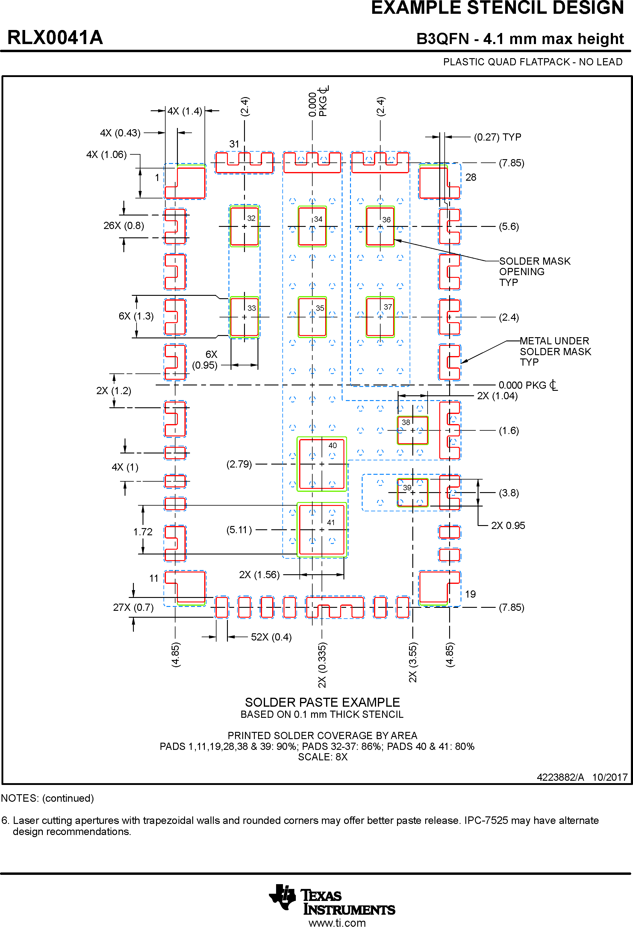
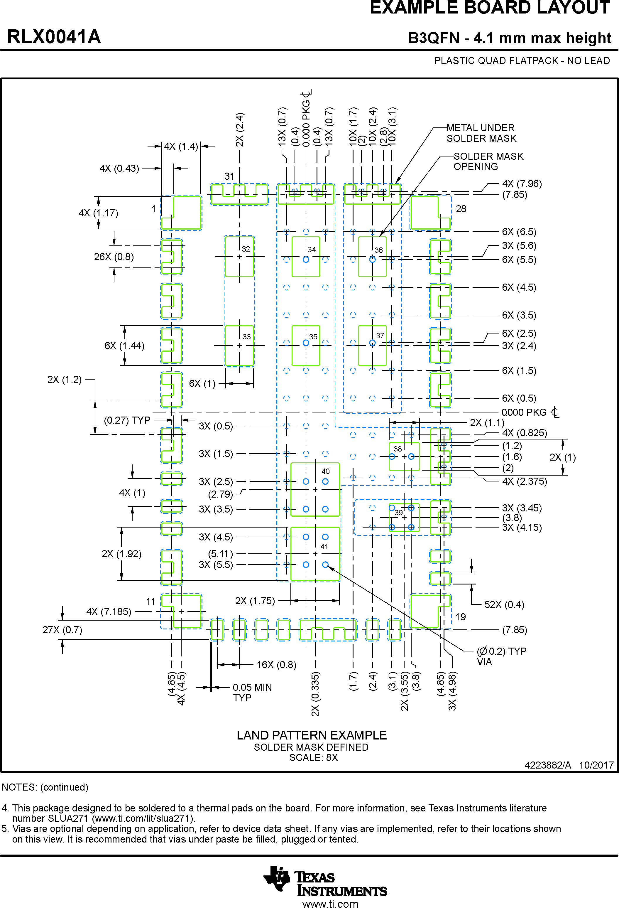
The following pages include mechanical packaging and orderable information. This information is the most current data available for the designated devices. This data is subject to change without notice and revision of this document. For browser-based versions of this data sheet, refer to the left-hand navigation.
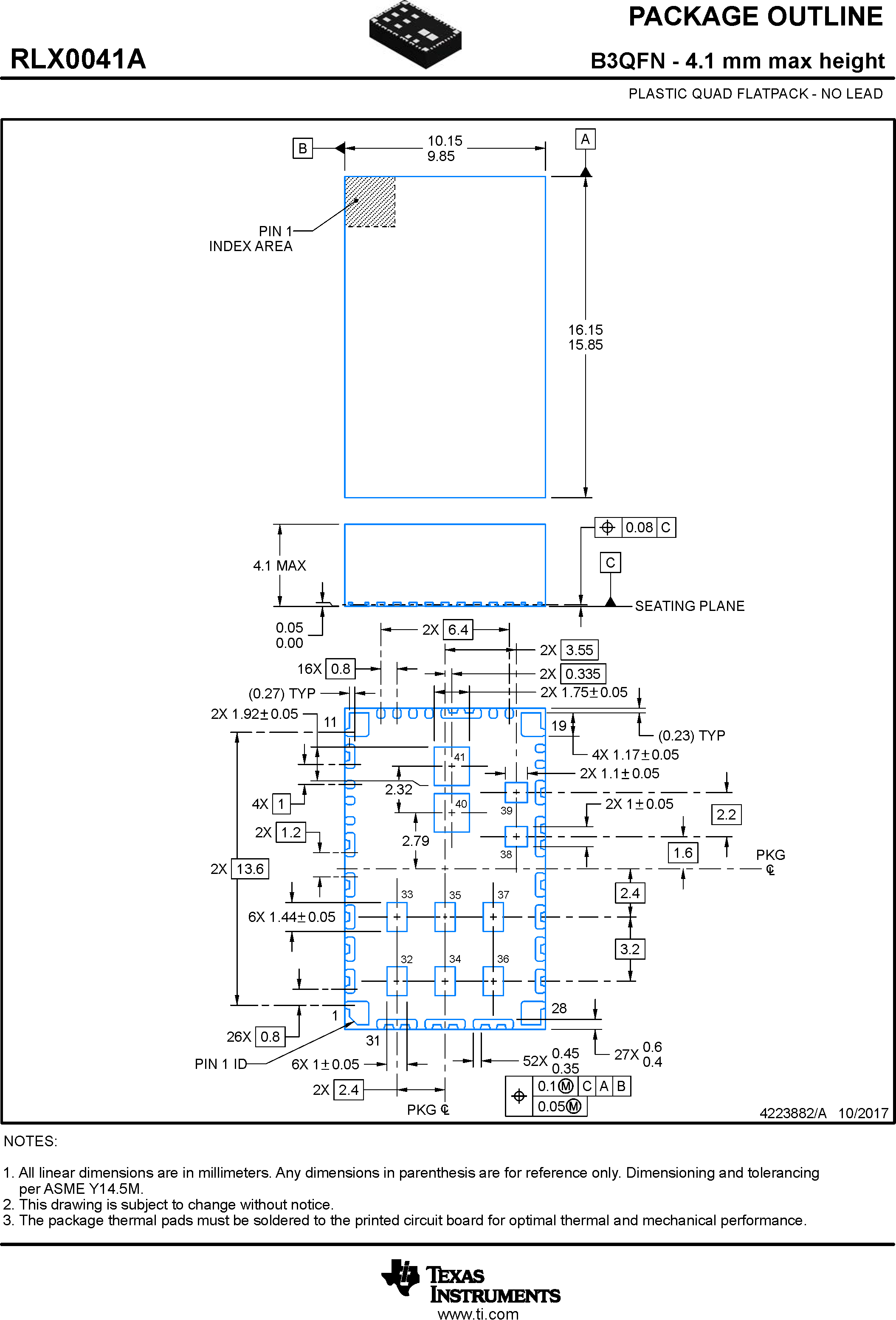
LMZM33604 LMZM33606-mechanical-drawing-01-snvsb11.png
LMZM33604 LMZM33606-mechanical-drawing-02-snvsb11.png
LMZM33604 LMZM33606-mechanical-drawing-03-snvsb11.png