SNVS311D May 2005 – February 2015 LP3878-ADJ
PRODUCTION DATA.
- 1 Features
- 2 Applications
- 3 Description
- 4 Revision History
- 5 Pin Configuration and Functions
- 6 Specifications
- 7 Detailed Description
- 8 Application and Implementation
- 9 Power Supply Recommendations
- 10Layout
- 11Device and Documentation Support
- 12Mechanical, Packaging, and Orderable Information
Package Options
Mechanical Data (Package|Pins)
Thermal pad, mechanical data (Package|Pins)
- DDA|8
Orderable Information
8 Application and Implementation
NOTE
Information in the following applications sections is not part of the TI component specification, and TI does not warrant its accuracy or completeness. TI’s customers are responsible for determining suitability of components for their purposes. Customers should validate and test their design implementation to confirm system functionality.
8.1 Application Information
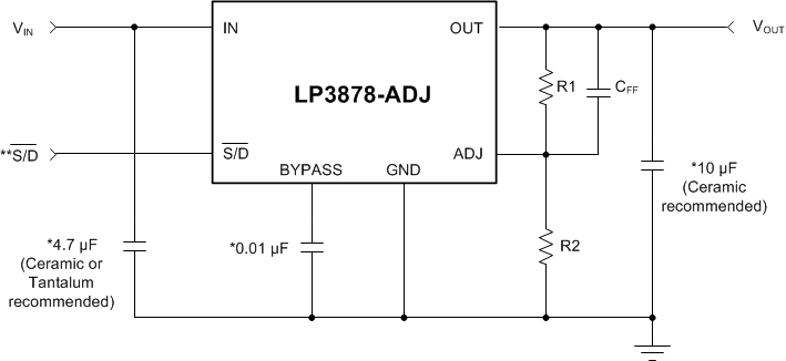
The LP3878-ADJ can provide 800-mA output current with 2.5-V to 6-V output voltage. A minimum 10-µF output capacitor is required for loop stability. An input capacitor of at least 4.7-µF is required also. The SHUTDOWN pin must be tied to input if not used. A 10-nF bypass capacitor is required to improve loop stability, it also can reduce noise on the regulator output significantly. A capacitor, CFF, is required to increase phase margin and assure loop stability. Output voltage can be set by two resistors R1 and R2 (see Figure 27), and R2 must be less than 5 kΩ to ensure loop stability.
8.2 Typical Application

**The SHUTDOWN (or S/D) pin must be actively terminated (see Device Functional Modes). Tie to IN (pin 4) if not used.
8.2.1 Design Requirements
| DESIGN PARAMETER | VALUE |
|---|---|
| Input voltage | 3.8 V ±10% |
| Output voltage | 1.8 V ±3% |
| Output current | 800 mA (maximum) |
| Input capacitor | 4.7 µF (minimum) |
| Output capacitor | 10 µF (minimum) |
| Bypass capacitor | 10 nF |
| External resistor R2 | 1 kΩ (less than 5 kΩ) |
8.2.2 Detailed Design Procedure
8.2.2.1 External Capacitors
Like any low-dropout regulator, the LP3878-ADJ requires external capacitors for regulator stability. These capacitors must be correctly selected for good performance.
8.2.2.1.1 Input Capacitor
A capacitor whose value is at least 4.7 µF (±20%) is required between the LP3878-ADJ input and ground. A good quality X5R or X7R ceramic capacitor should be used.
Capacitor tolerance and temperature variation must be considered when selecting a capacitor (see Capacitor Characteristics) to assure the minimum requirement of input capacitance is met over all operating conditions.
The input capacitor must be located not more than 0.5 inches from the input pin and returned to a clean analog ground. Any good quality ceramic or tantalum capacitor may be used, assuming the minimum input capacitance requirement is met.
8.2.2.1.2 Output Capacitor
The LP3878-ADJ requires a ceramic output capacitor whose size is at least 10 µF (±20%). A good quality X5R or X7R ceramic capacitor should be used. Capacitance tolerance and temperature characteristics must be considered when selecting an output capacitor.
The LP3878-ADJ is designed specifically to work with ceramic output capacitors, utilizing circuitry which allows the regulator to be stable across the entire range of output current with an ultra-low equivalent series resistance (ESR) output capacitor.
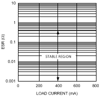
The output capacitor selected must meet the requirement for minimum amount of capacitance and also have an ESR value which is within the stable range. A curve is provided which shows the stable ESR range as a function of load current (see Figure 28).
 Figure 28. Stable Region for Output Capacitor ESR
NOTE
Important: The output capacitor must maintain its ESR within the stable region over the full operating temperature range of the application to assure stability.
The output capacitor ESR forms a zero which is required to add phase lead near the loop gain crossover frequency, typically in the range of 50 kHz to 200 kHz. The ESR at lower frequencies is of no importance. Some capacitor manufacturers list ESR at low frequencies only, and some give a formula for Dissipation Factor (DF) which can be used to calculate a value for a term referred to as ESR. However, because the DF formula is usually at a much lower frequency than the range listed above, it will give an unrealistically high value. If good quality X5R or X7R ceramic capacitors are used, the actual ESR in the 50-kHz to 200-kHz range will not exceed 25 mΩ. If these are used as output capacitors for the LP3878-ADJ, the regulator stability requirements are satisfied.
It is important to remember that capacitor tolerance and variation with temperature must be taken into consideration when selecting an output capacitor so that the minimum required amount of output capacitance is provided over the full operating temperature range (see Capacitor Characteristics).
The output capacitor must be located not more than 0.5 inches from the OUT pin and returned to a clean analog ground.
8.2.2.1.3 Noise Bypass Capacitor
The 10-nF capacitor on the BYPASS pin significantly reduces noise on the regulator output and is required for loop stability. However, the capacitor is connected directly to a high-impedance circuit in the bandgap reference.
Because this circuit has only a few µA flowing in it, any significant loading on this node will cause a change in the regulated output voltage. For this reason, dc leakage current through the noise bypass capacitor must never exceed 100 nA, and should be kept as low as possible for best output voltage accuracy.
The types of capacitors best suited for the noise bypass capacitor are ceramic and film. High-quality ceramic capacitors with either NPO or COG dielectric typically have very low leakage. 10-nF polypropylene and polycarbonate film capacitors are available in small surface-mount packages and typically have extremely low leakage current.
While the capacitor value on the BYPASS will affect start-up time, this is not intended to be used as a soft-start circuit. There is no dedicated discharge circuitry for this capacitor, and it can be pre-biased if the IN pin, or the SHUTDOWN pin are not at 0 V at start-up.
8.2.2.2 Feedforward Capacitor
The feedforward capacitor designated CFF in Figure 27 is required to increase phase margin and assure loop stability. Improved phase margin also gives better transient response to changes in load or input voltage, and faster settling time on the output voltage when transients occur. CFF forms both a pole and zero in the loop gain, the zero providing beneficial phase lead (which increases phase margin) and the pole adding undesirable phase lag (which should be minimized). The zero frequency is determined both by the value of CFF and R1:
The pole frequency resulting from CFF is determined by the value of CFF and the parallel combination of R1 and R2:
At higher output voltages where R1 is much greater than R2, the value of R2 primarily determines the value of the parallel combination of R1 // R2. This puts the pole at a much higher frequency than the zero. As the regulated output voltage is reduced (and the value of R1 decreases), the parallel effect of R2 diminishes and the two equations become equal (at which point the pole and zero cancel out). Because the pole frequency gets closer to the zero at lower output voltages, the beneficial effects of CFF are increased if the frequency range of the zero is shifted slightly higher for applications with low VOUT (because then the pole adds less phase lag at the loop crossover frequency).
CFF should be selected to place the pole-zero pair at a frequency where the net phase lead added to the loop at the crossover frequency is maximized. The following design guidelines were obtained from bench testing to optimize phase margin, transient response, and settling time:
- For VOUT ≤ 2.5 V: CFF should be selected to set the zero frequency in the range of about 50 kHz to 200 kHz.
- For VOUT > 2.5 V: CFF should be selected to set the zero frequency in the range of about 20 kHz to 100 kHz.
8.2.2.3 Capacitor Characteristics
8.2.2.3.1 Ceramic
The LP3878-ADJ was designed to work with ceramic capacitors on the output to take advantage of the benefits they offer: for capacitance values in the 10-µF range, ceramics are the least expensive and also have the lowest ESR values (which makes them best for eliminating high-frequency noise). The ESR of a typical 10-µF ceramic capacitor is in the range of 5 mΩ to 10 mΩ, which meets the ESR limits required for stability by the LP3878-ADJ.
One disadvantage of ceramic capacitors is that their capacitance can vary with temperature. Many large value ceramic capacitors (≥ 2.2 µF) are manufactured with the Z5U or Y5V temperature characteristic, which results in the capacitance dropping by more than 50% as the temperature goes from 25°C to 85°C.
Another significant problem with Z5U and Y5V dielectric devices is that the capacitance drops severely with applied voltage. A typical Z5U or Y5V capacitor can lose 60% of its rated capacitance with half of the rated voltage applied to it.
For these reasons, X7R and X5R type ceramic capacitors must be used on the input and output of the LP3878-ADJ.
8.2.2.4 Setting the Output Voltage
The output voltage is set using resistors R1 and R2 (see Figure 27).
The formula for output voltage is:
R2 must be less than 5 kΩ to ensure loop stability.
To prevent voltage errors, R1 and R2 must be located near the LP3878-ADJ and connected via traces with no other currents flowing in them (Kelvin connect). The bottom of the R1/R2 divider must be connected directly to the LP3878-ADJ ground pin.
8.2.3 Application Curves
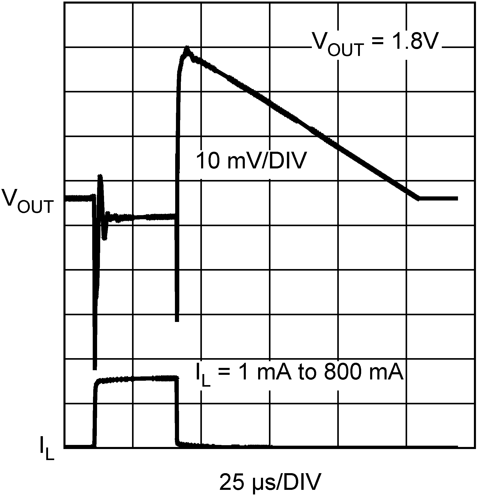
 Figure 29. Load Transient Response
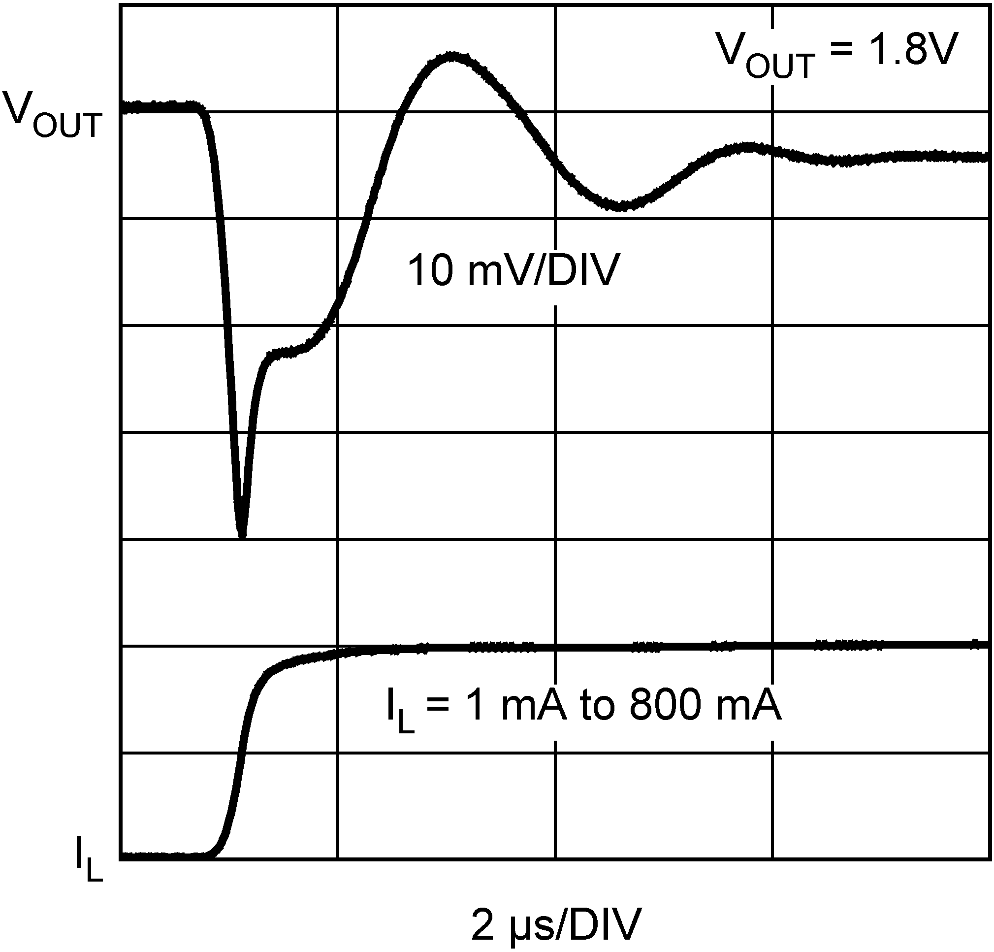
 Figure 30. Load Transient Response