SNVS311D May 2005 – February 2015 LP3878-ADJ
PRODUCTION DATA.
- 1 Features
- 2 Applications
- 3 Description
- 4 Revision History
- 5 Pin Configuration and Functions
- 6 Specifications
- 7 Detailed Description
- 8 Application and Implementation
- 9 Power Supply Recommendations
- 10Layout
- 11Device and Documentation Support
- 12Mechanical, Packaging, and Orderable Information
Package Options
Mechanical Data (Package|Pins)
Thermal pad, mechanical data (Package|Pins)
- DDA|8
Orderable Information
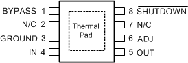
5 Pin Configuration and Functions
SO PowerPAD (DDA) Package
8-Pin
Top View
WSON (NGT) Package
8-Pin
Top View
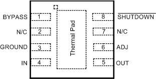
Pin Functions
| PIN | I/O | DESCRIPTION | |
|---|---|---|---|
| NAME | NUMBER | ||
| ADJ | 6 | I | Provides feedback to error amplifier from the resistive divider that sets the output voltage. |
| BYPASS | 1 | — | The capacitor connected between BYPASS and GROUND lowers output noise voltage level and is required for loop stability. |
| GROUND | 3 | — | Device ground. |
| IN | 4 | I | Input source voltage. |
| N/C | 2 | DO NOT CONNECT. Device pin 2 is reserved for post packaging test and calibration of the LP3878-ADJ VADJ accuracy. This pin must be left floating. Do not connect to any potential. Do not connect to ground. Any attempt to do pin continuity testing on device pin 2 is discouraged. Continuity test results will be variable depending on the actions of the factory calibration. Aggressive pin continuity testing (high voltage, or high current) on device pin 2 may activate the trim circuitry forcing VADJ to move out of tolerance. | |
| N/C | 7 | No internal connection. | |
| OUT | 5 | O | Regulated output voltage. |
| SHUTDOWN | 8 | I | Output is enabled above turnon threshold voltage. Pull down to turn off regulator output. |
| Thermal Pad | — | — | The exposed thermal pad on the bottom of the package should be connected to a copper thermal pad on the PCB under the package. The use of thermal vias to remove heat from the package into the PCB is recommended. Connect the thermal pad to ground potential or leave floating. Do not connect the thermal pad to any potential other than the same ground potential seen at device pin 3. For additional information on using TI's Non Pull Back WSON package, see Application Note AN-1187, SNOA401. |