SNVS311D May 2005 – February 2015 LP3878-ADJ
PRODUCTION DATA.
- 1 Features
- 2 Applications
- 3 Description
- 4 Revision History
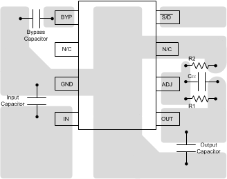
- 5 Pin Configuration and Functions
- 6 Specifications
- 7 Detailed Description
- 8 Application and Implementation
- 9 Power Supply Recommendations
- 10Layout
- 11Device and Documentation Support
- 12Mechanical, Packaging, and Orderable Information
Package Options
Mechanical Data (Package|Pins)
Thermal pad, mechanical data (Package|Pins)
- DDA|8
Orderable Information
10 Layout
10.1 Layout Guidelines
Good PC layout practices must be used or instability can be induced because of ground loops and voltage drops. The input and output capacitors must be directly connected to the input, output, and ground pins of the regulator using traces which do not have other currents flowing in them (Kelvin connect).
The best way to do this is to lay out CIN and COUT near the device with short traces to the IN, OUT, and ground pins. The regulator ground pin should be connected to the external circuit ground so that the regulator and its capacitors have a single point ground.
It should be noted that stability problems have been seen in applications where vias to an internal ground plane were used at the ground points of the IC and the input and output capacitors. This was caused by varying ground potentials at these nodes resulting from current flowing through the ground plane. Using a single-point ground technique for the regulator and its capacitors fixed the problem.
Because high current flows through the traces going into IN and coming from OUT, Kelvin connect the capacitor leads to these pins so there is no voltage drop in series with the input and output capacitors.
10.2 Layout Example
10.3 Power Dissipation
The LP3878-ADJ is offered in the 8-lead SO PowerPAD or WSON surface-mount packages to allow for increased power dissipation compared to the SO-8 and Mini SO-8. For details on thermal performance as well as mounting and soldering specifications, refer to Application Note AN-1187, SNOA401.