SNVS251J May 2004 – September 2014 LP3990
PRODUCTION DATA.
- 1 Features
- 2 Applications
- 3 Description
- 4 Revision History
- 5 Pin Configuration and Functions
- 6 Specifications
- 7 Detailed Description
- 8 Application and Implementation
- 9 Power Supply Recommendations
- 10Layout
- 11Device and Documentation Support
- 12Mechanical, Packaging, and Orderable Information
Package Options
Mechanical Data (Package|Pins)
Thermal pad, mechanical data (Package|Pins)
Orderable Information
1 Features
- 1% Voltage Accuracy at Room Temperature
- Stable with Ceramic Capacitor
- Logic Controlled Enable
- No Noise Bypass Capacitor Required
- Thermal-Overload and Short-Circuit Protection
- Input Voltage Range, 2 V to 6 V
- Output Voltage Range, 0.8 V to 3.3 V
- Output Current, 150 mA
- Output Stable - Capacitors, 1 µF
- Virtually Zero IQ (Disabled), < 10 nA
- Very Low IQ (Enabled), 43 µA
- Low Output Noise, 150 µVRMS
- PSRR, 55 dB at 1 kHz
- Fast Start-Up, 105 µs
2 Applications
- Cellular Handsets
- Hand-Held Information Appliances
3 Description
The LP3990 regulator is designed to meet the requirements of portable, battery-powered systems providing an accurate output voltage, low-noise, and low-quiescent current. The LP3990 will provide a 0.8-V output from the low input voltage of 2 V at up to a 150-mA load current. When switched into shutdown mode via a logic signal at the enable pin (EN), the power consumption is reduced to virtually zero.
The LP3990 is designed to be stable with space-saving ceramic capacitors with values as low as 1 µF.
Performance is specified for a –40°C to 125°C junction temperature range.
For output voltages other than 0.8 V, 1.2 V, 1.35 V, 1.5 V, 1.8 V, 2.5 V, 2.8 V, or 3.3 V, please contact the Texas Instruments sales office.
Device Information(1)
| PART NUMBER | PACKAGE | BODY SIZE (NOM) |
|---|---|---|
| LP3990 | DSBGA (4) | 1.324 mm x 1.045 mm (MAX) |
| WSON (6) | 2.90 mm x 1.60 mm | |
| SOT-23 (5) | 3.00 mm x 3.00 mm |
- For all available packages, see the orderable addendum at the end of the datasheet.
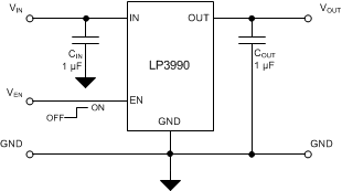
Simplified Schematic