SNVS251J May 2004 – September 2014 LP3990
PRODUCTION DATA.
- 1 Features
- 2 Applications
- 3 Description
- 4 Revision History
- 5 Pin Configuration and Functions
- 6 Specifications
- 7 Detailed Description
- 8 Application and Implementation
- 9 Power Supply Recommendations
- 10Layout
- 11Device and Documentation Support
- 12Mechanical, Packaging, and Orderable Information
Package Options
Mechanical Data (Package|Pins)
Thermal pad, mechanical data (Package|Pins)
Orderable Information
7 Detailed Description
7.1 Overview
Designed meet the requirements of portable, battery-powered digital systems providing an accurate output voltage with fast start-up. When disabled via a low logic signal at the enable pin (EN), the power consumption is reduced to virtually zero
The LP3990 is designed to perform with a single 1-μF input capacitor and a single 1-μF ceramic output capacitor.
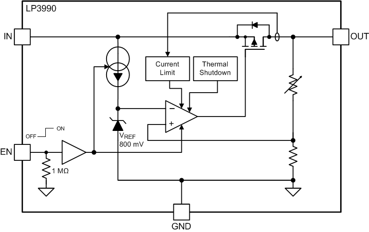
7.2 Functional Block Diagram
7.3 Feature Description
7.3.1 Enable (EN)
The LP3990 Enable (EN) pin is internally held low by a 1-MΩ resistor to GND. The EN pin voltage must be higher than the VIH threshold to ensure that the device is fully enabled under all operating conditions. The EN pin voltage must be lower than the VIL threshold to ensure that the device is fully disabled. If the EN pin is left open the LP3990 output will be disabled.
7.3.2 Thermal Overload Protection (TSD)
Thermal Shutdown disables the output when the junction temperature rises to approximately 155°C which allows the device to cool. When the junction temperature cools to approximately 140°C, the output circuitry enables. Based on power dissipation, thermal resistance, and ambient temperature, the thermal protection circuit may cycle on and off. This thermal cycling limits the dissipation of the regulator and protects it from damage as a result of overheating.
The Thermal Shutdown circuitry of the LP3990 has been designed to protect against temporary thermal overload conditions. The Thermal Shutdown circuitry was not intended to replace proper heat-sinking. Continuously running the LP3990 device into thermal shutdown may degrade device reliability.
7.4 Device Functional Modes
7.4.1 Enable (EN)
The LP3990 EN pin is internally held low by a 1-MΩ resistor to GND. The EN pin voltage must be higher than the VIH threshold to ensure that the device is fully enabled under all operating conditions.
7.4.2 Minimum Operating Input Voltage (VIN)
The LP3990 does not include any dedicated UVLO circuitry. The LP3990 internal circuitry is not fully functional until VIN is at least 2 V. The output voltage is not regulated until VIN ≥ (VOUT + VDO), or 2 V, whichever is higher.