SNVS251J May 2004 – September 2014 LP3990
PRODUCTION DATA.
- 1 Features
- 2 Applications
- 3 Description
- 4 Revision History
- 5 Pin Configuration and Functions
- 6 Specifications
- 7 Detailed Description
- 8 Application and Implementation
- 9 Power Supply Recommendations
- 10Layout
- 11Device and Documentation Support
- 12Mechanical, Packaging, and Orderable Information
Package Options
Mechanical Data (Package|Pins)
Thermal pad, mechanical data (Package|Pins)
Orderable Information
6 Specifications
6.1 Absolute Maximum Ratings(1)(2)(3)
over operating free-air temperature range (unless otherwise noted)| MIN | MAX | UNIT | ||
|---|---|---|---|---|
| Input voltage | –0.3 | 6.5 | V | |
| Output voltage | –0.3 | Note(4) | ||
| ENABLE input voltage | –0.3 | 6.5 | ||
| Continuous power dissipation internally limited | Note(5) | |||
(1) Stresses beyond those listed under Absolute Maximum Ratings may cause permanent damage to the device. These are stress ratings only, which do not imply functional operation of the device at these or any other conditions beyond those indicated under Recommended Operating Conditions. Exposure to absolute-maximum-rated conditions for extended periods may affect device reliability.
(2) If Military/Aerospace specified devices are required, please contact the TI Sales Office/Distributors for availability and specifications.
(3) All voltages are with respect to the potential at the GND pin.
(4) The lower of VIN + 0.3 V or 6.5 V.
(5) Internal thermal shutdown circuitry protects the device from permanent damage.
6.2 Handling Ratings
| MIN | MAX | UNIT | |||
|---|---|---|---|---|---|
| Tstg | Storage temperature range | –65 | 150 | °C | |
| V(ESD) | Electrostatic discharge | Human body model (HBM), per ANSI/ESDA/JEDEC JS-001, all pins(1) | –2000 | 2000 | V |
| Charged device model (CDM), per JEDEC specification JESD22-C101, all pins | 250 | 1500 | |||
| Machine model | –200 | 200 | |||
(1) JEDEC document JEP155 states that 2000-V HBM allows safe manufacturing with a standard ESD control process.
6.3 Recommended Operating Conditions
over operating free-air temperature range (unless otherwise noted)| MIN | NOM | MAX | UNIT | ||
|---|---|---|---|---|---|
| Input voltage, VIN | 2 | 6 | V | ||
| Enable input voltage, VEN | 0.0 | VIN | |||
| Junction temperature, TJ(1) | –40 | 125 | °C | ||
(1) TJ(max) = (TA(max) + (RθJA × PD(max)) )
6.4 Thermal Information
| THERMAL METRIC(1) | LP3990 | UNIT | |||
|---|---|---|---|---|---|
| YZR (DSBGA) | DBV (SOT-23) | NGG (WSON) | |||
| 4 PINS | 5 PINS | 6 PINS | |||
| RθJA | Junction-to-ambient thermal resistance | 188.9 | 165.2 | 53.9 | °C/W |
| RθJC(top) | Junction-to-case (top) thermal resistance | 1.0 | 69.9 | 51.2 | |
| RθJB | Junction-to-board thermal resistance | 105.3 | 27.3 | 28.2 | |
| ψJT | Junction-to-top characterization parameter | 0.7 | 1.8 | 0.6 | |
| ψJB | Junction-to-board characterization parameter | 105.2 | 26.8 | 28.3 | |
| RθJC(bot) | Junction-to-case (bottom) thermal resistance | N/A | N/A | 8.1 | |
(1) For more information about traditional and new thermal metrics, see the IC Package Thermal Metrics application report, SPRA953.
6.5 Electrical Characteristics(1)(3)
Unless otherwise noted, VEN = 950 mV, VIN = VOUT + 1 V or VIN = 2 V, whichever is higher. CIN = 1 µF, IOUT = 1 mA, COUT = 0.47 µF.| PARAMETER | TEST CONDITIONS | MIN | TYP | MAX | UNIT | ||
|---|---|---|---|---|---|---|---|
| VIN | Input voltage | Note (2), TJ = 25°C | 2 | 6 | V | ||
| ΔVOUT | Output voltage tolerance | ILOAD = 1 mA TJ = 25°C |
DSBGA | –1 | 1% | ||
| WQFN | –1.5% | 1.5% | |||||
| SOT-23 | –1.5% | 1.5% | |||||
| Over full line and load regulation | DSBGA | –2.5% | 2.5% | ||||
| WQFN | –3% | 3% | |||||
| SOT-23 | –4% | 4% | |||||
| Line regulation error | VIN = (VOUT(NOM) + 1 V) to 6 V | 0.1 | 0.02 | 0.1 | %/V | ||
| Load regulation error | IOUT = 1 mA to 150 mA |
VOUT = 0.8 V to 1.95 V DSBGA |
–0.005 | 0.002 | 0.005 | %/mA | |
| VOUT = 0.8 V to 1.95 V WQFN, SOT-23 |
–0.008 | 0.003 | 0.008 | ||||
| VOUT = 2 V to 3.3 V DSBGA |
–0.002 | 0.0005 | 0.002 | ||||
| VOUT = 2 V to 3.3 V WQFN, SOT-23 |
–0.005 | 0.002 | 0.005 | ||||
| VDO | Dropout voltage | IOUT = 150 mA(4)(5) | 120 | 200 | mV | ||
| ILOAD | Load current | Note (5)(6), TJ = 25°C | 0 | µA | |||
| IQ | Quiescent current | VEN = 950 mV, IOUT = 0 mA | 43 | 80 | µA | ||
| VEN = 950 mV, IOUT = 150 mA | 65 | 120 | |||||
| VEN = 0.4 V (output disabled), TJ = 25°C | 0.002 | 0.2 | |||||
| ISC | Short circuit current limit | Note (7) | 550 | 1000 | mA | ||
| IOUT | Maximum output current | 150 | |||||
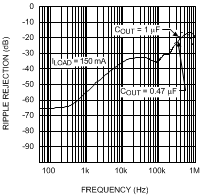
| PSRR | Power Supply Rejection Ratio | ƒ = 1 kHz, IOUT = 1 mA to 150 mA | 55 | dB | |||
| ƒ = 10 kHz, IOUT = 150 mA | 35 | ||||||
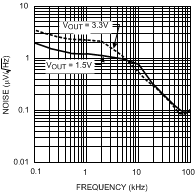
| eη | Output noise voltage(5) | BW = 10 Hz to 100 kHz | VOUT = 0.8 V | 60 | µVRMS | ||
| VOUT = 1.5 V | 125 | ||||||
| VOUT = 3.3 V | 180 | ||||||
| TSHUTDOWN | Thermal shutdown junction temperature | Junction temperature (TJ) rising until the output is disabled | 155 | °C | |||
| Hysteresis | 15 | ||||||
| ENABLE CONTROL CHARACTERISTICS | |||||||
| IEN(8) | Maximum input current at EN pin | VEN = 0 V (Output is disabled) TJ = 25°C |
0.001 | 0.1 | µA | ||
| VEN = 6 V | 2.5 | 6 | 10 | ||||
| VIL | Low input threshold | VIN = 2 V to 6 V VEN falling from ≥ VIH until the output is disabled |
0.4 | V | |||
| VIH | High input threshold | VIN = 2 V to 6 V VEN rising from ≤ VIL until the output is enabled |
0.95 | ||||
(1) All voltages are with respect to the device GND terminal, unless otherwise stated.
(2) VIN(MIN) = VOUT(NOM) + 0.5 V, or 2 V, whichever is higher.
(3) Minimum and Maximum limits are ensured through test, design, or statistical correlation over the operating junction temperature range (TJ) of –40°C to 125°C, unless otherwise stated. Typical values represent the most likely parametric norm at TJ = 25°C, and are provided for reference purposes only.
(4) Dropout voltage is voltage difference between input and output at which the output voltage drops to 100 mV below its nominal value. This parameter applies only for output voltages above 2 V.
(5) This electrical specification is verified by design.
(6) The device maintains the regulated output voltage without the load.
(7) Short-circuit current is measured with VOUT pulled to 0 V and VIN worst case = 6 V.
(8) ENABLE Pin has 1-MΩ (typical) resistor connected to GND.
6.6 Output Capacitor, Recommended Specifications(1)
| PARAMETER | TEST CONDITIONS | MIN | TYP | MAX | UNIT | |
|---|---|---|---|---|---|---|
| COUT | Output capacitance | Capacitance(3) | 0.7(2) | 1 | 500 | µF |
| ESR | 5 | mΩ | ||||
(1) Unless otherwise specified, values and limits apply for TJ = 25°C.
(2) Limit applies over the full operating junction temperature range (TJ) of −40°C to 125°C.
(3) The full operating conditions for the application should be considered when selecting a suitable capacitor to ensure that the minimum value of capacitance is always met. Recommended capacitor type is X7R. However, dependent on application, X5R, Y5V, and Z5U can also be used. (See Detailed Design Procedure.)
6.7 Timing Requirements
| MIN | NOM(1) | MAX(2) | UNIT | ||||
|---|---|---|---|---|---|---|---|
| TON | Turnon time (3) | From VEN ↑ VIH to VOUT 95% level (VIN(MIN) to 6 V) |
VOUT = 0.8 V | 80 | 150 | µs | |
| VOUT = 1.5 V | 105 | 200 | |||||
| VOUT = 3.3 V | 175 | 250 | |||||
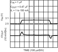
| Transient response | Line transient response (ΔVOUT) | Trise = Tfall = 30 µs(3), ΔVIN = 600 mV |
8 | 16 | mV (pk-pk) | ||
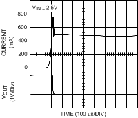
| Load transient response (ΔVOUT) | Trise = Tfall = 1 µs(3), IOUT = 1 mA to 150 mA COUT = 1 µF |
55 | 100 | mV | |||
(1) Nom values apply for TJ = 25°C.
(2) Maximum limits apply over the full operating junction temperature (TJ) range of −40°C to 125°C.
(3) This electrical specification is verified by design.
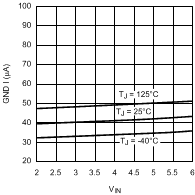
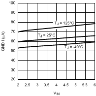
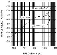
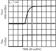
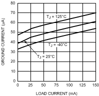
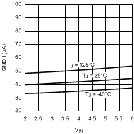
6.8 Typical Performance Characteristics
Unless otherwise specified, CIN = 1 µF ceramic, COUT = 0.47 µF ceramic, VIN = VOUT(NOM) + 1 V, TA = 25°C, VOUT(NOM) = 1.5 V; VEN = VIN.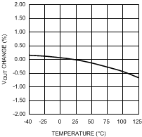
| ILOAD = 0 mA | ||
| ILOAD = 150 mA | ||
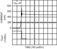
| ILOAD = 1 mA | ||