SNVS251J May 2004 – September 2014 LP3990
PRODUCTION DATA.
- 1 Features
- 2 Applications
- 3 Description
- 4 Revision History
- 5 Pin Configuration and Functions
- 6 Specifications
- 7 Detailed Description
- 8 Application and Implementation
- 9 Power Supply Recommendations
- 10Layout
- 11Device and Documentation Support
- 12Mechanical, Packaging, and Orderable Information
Package Options
Mechanical Data (Package|Pins)
Thermal pad, mechanical data (Package|Pins)
Orderable Information
10 Layout
10.1 Layout Guidelines
The dynamic performance of the LP3990 is dependant on the layout of the PCB. PCB layout practices that are adequate for typical LDO's may degrade the load regulation, PSRR, noise, or transient performance of the LP3990.
Best performance is achieved by placing CIN and COUT on the same side of the PCB as the LP3990, and as close as is practical to the package. The ground connections for CIN and COUT should be back to the LP3990 ground pin using as wide, and as short, of a copper trace as is practical.
Connections using long trace lengths, narrow trace widths, and/or connections through vias should be avoided. These will add parasitic inductances and resistance that results in inferior performance especially during transient conditions.
A Ground Plane, either on the opposite side of a two-layer PCB, or embedded in a multi-layer PCB, is strongly recommended. This Ground Plane serves two purposes : 1) Provide a circuit reference plane to assure accuracy, and 2) provides a thermal plane to remove heat from the LP3990 WSON package through thermal vias under the package DAP.
10.2 Layout Examples
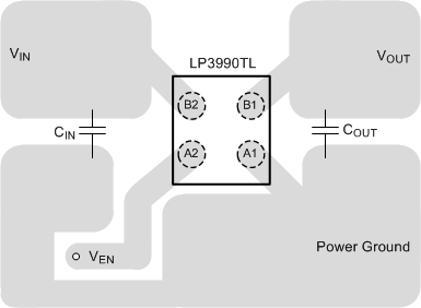 Figure 17. LP3990 DSBGA Layout
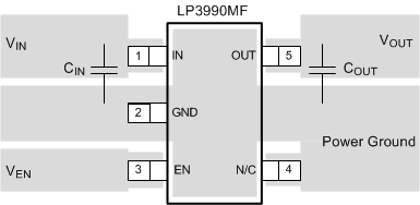 Figure 18. LP3990 SOT-23 Layout
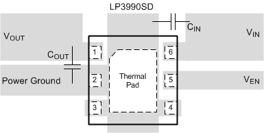 Figure 19. LP3990 WSON Layout
10.3 DSBGA Mounting
The DSBGA package requires specific mounting techniques, which are detailed in TI Application Note DSBGA Wafer Level Chip Scale PackageSNVA009.
For best results during assembly, alignment ordinals on the PC board may be used to facilitate placement of the DSBGA device.
10.4 DSBGA Light Sensitivity
Exposing the DSBGA device to direct light may affect the operation of the device. Light sources, such as halogen lamps, can affect electrical performance, if placed in close proximity to the device.
Light with wavelengths in the infra-red portion of the spectrum is the most detrimental, and so, fluorescent lighting used inside most buildings, has little or no effect on performance.