SLVSEM4B June 2018 – April 2021 LSF0204-Q1
PRODUCTION DATA
- 1 Features
- 2 Applications
- 3 Description
- 4 Revision History
- 5 Pin Configuration and Functions
-
6 Specifications
- 6.1 Absolute Maximum Ratings
- 6.2 ESD Ratings
- 6.3 Recommended Operating Conditions
- 6.4 Thermal Information
- 6.5 Electrical Characteristics
- 6.6 Switching Characteristics: AC Performance (Translating Down, 3.3 V to 1.8 V)
- 6.7 Switching Characteristics: AC Performance (Translating Down, 3.3 V to 1.2 V)
- 6.8 Switching Characteristics: AC Performance (Translating Up, 1.8 V to 3.3 V)
- 6.9 Switching Characteristics: AC Performance (Translating Up, 1.2 V to 1.8 V)
- 6.10 Typical Characteristics
- 7 Detailed Description
- 8 Application and Implementation
- 9 Power Supply Recommendations
- 10Layout
- 11Device and Documentation Support
- 12Mechanical, Packaging, and Orderable Information
Package Options
Mechanical Data (Package|Pins)
- PW|14
Thermal pad, mechanical data (Package|Pins)
Orderable Information
3 Description
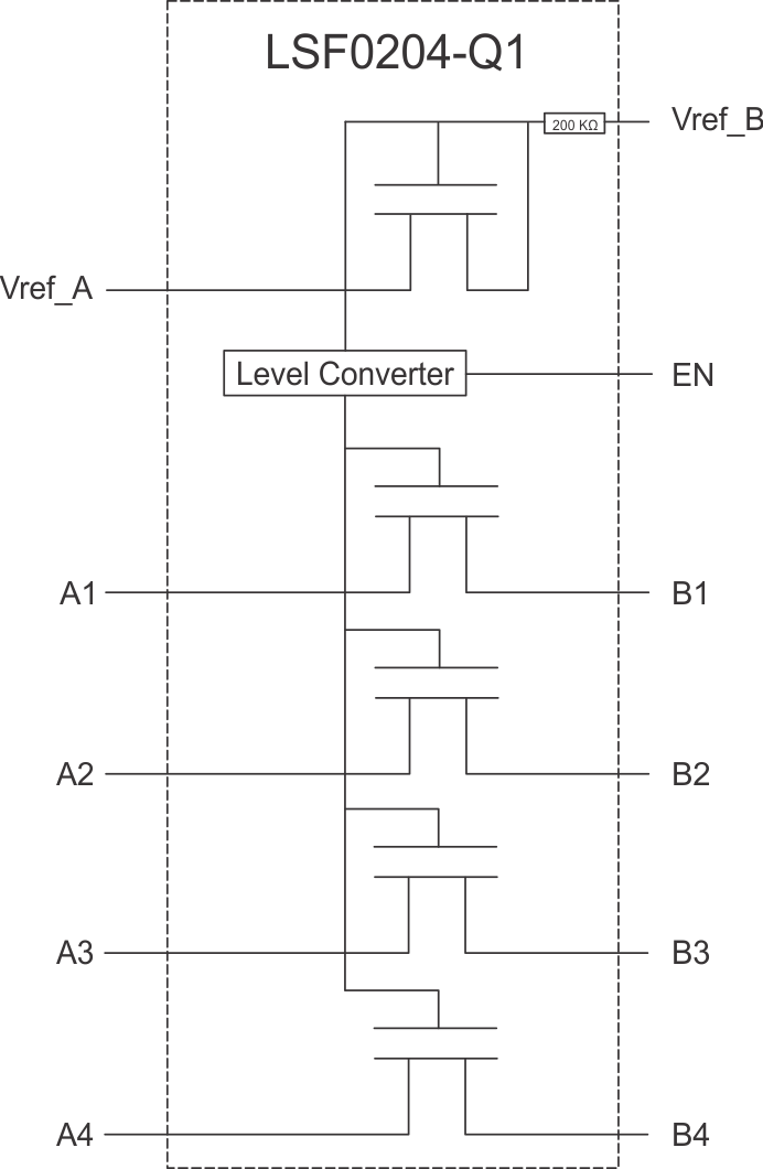
The LSF0204-Q1 is automotive qualified four channel auto bidirectional voltage translator that operate from 0.8 V to 4.5 V (Vref_A) and 1.8 V to 5.5 V (Vref_B). This range allows for bidirectional voltage translations between 0.8 V and 5.5 V without the need for a direction pin.
When the An or Bn port is LOW, the switch is in the ON-state and a low resistance connection exists between the An and Bn ports. The low Ron of the switch allows connections to be made with minimal propagation delay and minimal signal distortion. The voltage on the A or B side will be limited to Vref_A and can be pulled up to any level between Vref_A and 5.5 V
The supply voltage (VPUn) for each channel may be individually set up with a pull up resistor. For example, CH1 may be used in up-translation mode (1.2 V ↔ 3.3 V) and CH2 in down-translation mode (2.5 V ↔ 1.8 V).
When EN is HIGH, the translator switch is on, and the An I/O is connected to the Bn I/O, respectively, allowing bidirectional data flow between ports. When EN is LOW, the translator switch is off, and a high-impedance state exists between ports. The EN input circuit is designed to be supplied by Vref_A. EN must be LOW to ensure the high-impedance state during power-up or power-down.
| PART NUMBER | PACKAGE | BODY SIZE (NOM) |
|---|---|---|
| LSF0204QPWRQ1 | TSSOP (14) | 5.00 mm × 4.40 mm |
 Simplified Schematic