SLASE58E February 2016 – December 2019 MSP430FR2310 , MSP430FR2311
PRODUCTION DATA.
- 1Device Overview
- 2Revision History
- 3Device Comparison
- 4Terminal Configuration and Functions
-
5Specifications
- 5.1 Absolute Maximum Ratings
- 5.2 ESD Ratings
- 5.3 Recommended Operating Conditions
- 5.4 Active Mode Supply Current Into VCC Excluding External Current
- 5.5 Active Mode Supply Current Per MHz
- 5.6 Low-Power Mode LPM0 Supply Currents Into VCC Excluding External Current
- 5.7 Low-Power Mode LPM3 and LPM4 Supply Currents (Into VCC) Excluding External Current
- 5.8 Low-Power Mode LPMx.5 Supply Currents (Into VCC) Excluding External Current
- 5.9 Production Distribution of LPM Supply Currents
- 5.10 Typical Characteristics – Current Consumption Per Module
- 5.11 Thermal Resistance Characteristics
- 5.12
Timing and Switching Characteristics
- 5.12.1 Power Supply Sequencing
- 5.12.2 Reset Timing
- 5.12.3 Clock Specifications
- 5.12.4 Digital I/Os
- 5.12.5 VREF+ Built-in Reference
- 5.12.6 Timer_B
- 5.12.7
eUSCI
- Table 5-14 eUSCI (UART Mode) Clock Frequency
- Table 5-15 eUSCI (UART Mode) Switching Characteristics
- Table 5-16 eUSCI (SPI Master Mode) Clock Frequency
- Table 5-17 eUSCI (SPI Master Mode) Switching Characteristics
- Table 5-18 eUSCI (SPI Slave Mode) Switching Characteristics
- Table 5-19 eUSCI (I2C Mode) Switching Characteristics
- 5.12.8 ADC
- 5.12.9 Enhanced Comparator (eCOMP)
- 5.12.10 Smart Analog Combo (SAC)
- 5.12.11 Transimpedance Amplifier (TIA)
- 5.12.12 FRAM
- 5.12.13 Emulation and Debug
-
6Detailed Description
- 6.1 Overview
- 6.2 CPU
- 6.3 Operating Modes
- 6.4 Interrupt Vector Addresses
- 6.5 Memory Organization
- 6.6 Bootloader (BSL)
- 6.7 JTAG Standard Interface
- 6.8 Spy-Bi-Wire Interface (SBW)
- 6.9 FRAM
- 6.10 Memory Protection
- 6.11
Peripherals
- 6.11.1 Power-Management Module (PMM) and On-chip Reference Voltages
- 6.11.2 Clock System (CS) and Clock Distribution
- 6.11.3 General-Purpose Input/Output Port (I/O)
- 6.11.4 Watchdog Timer (WDT)
- 6.11.5 System Module (SYS)
- 6.11.6 Cyclic Redundancy Check (CRC)
- 6.11.7 Enhanced Universal Serial Communication Interface (eUSCI_A0, eUSCI_B0)
- 6.11.8 Timers (Timer0_B3, Timer1_B3)
- 6.11.9 Backup Memory (BAKMEM)
- 6.11.10 Real-Time Clock (RTC) Counter
- 6.11.11 10-Bit Analog-to-Digital Converter (ADC)
- 6.11.12 eCOMP0
- 6.11.13 SAC0
- 6.11.14 TIA0
- 6.11.15 eCOMP0, SAC0, TIA0, and ADC in SOC Interconnection
- 6.11.16 Embedded Emulation Module (EEM)
- 6.11.17 Peripheral File Map
- 6.12 Input/Output Diagrams
- 6.13 Device Descriptors (TLV)
- 6.14 Identification
- 7Applications, Implementation, and Layout
- 8Device and Documentation Support
- 9Mechanical, Packaging, and Orderable Information
Package Options
Mechanical Data (Package|Pins)
Thermal pad, mechanical data (Package|Pins)
- RGY|16
Orderable Information
7.1.3 JTAG
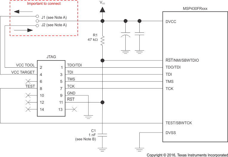
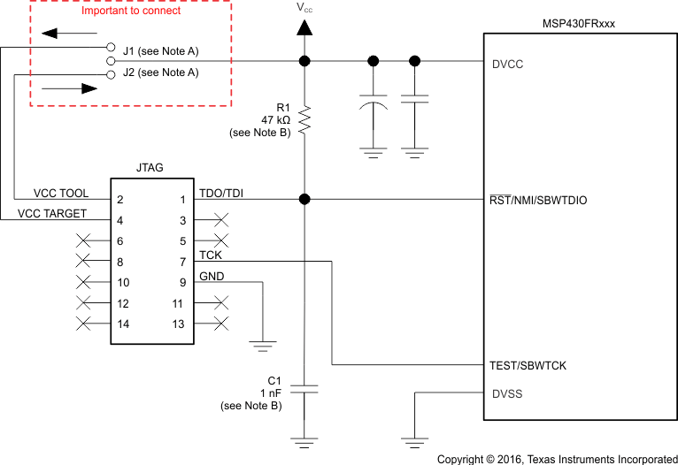
With the proper connections, the debugger and a hardware JTAG interface (such as the MSP-FET or MSP-FET430UIF) can be used to program and debug code on the target board. In addition, the connections also support the MSP-GANG production programmers, thus providing an easy way to program prototype boards, if desired. Figure 7-3 shows the connections between the 14-pin JTAG connector and the target device required to support in-system programming and debugging for 4-wire JTAG communication. Figure 7-4 shows the connections for 2-wire JTAG mode (Spy-Bi-Wire).
The connections for the MSP-FET and MSP-FET430UIF interface modules and the MSP-GANG are identical. Both can supply VCC to the target board (through pin 2). In addition, the MSP-FET and MSP-FET430UIF interface modules and MSP-GANG have a VCC sense feature that, if used, requires an alternate connection (pin 4 instead of pin 2). The VCC-sense feature detects the local VCC present on the target board (that is, a battery or other local power supply) and adjusts the output signals accordingly. Figure 7-3 and Figure 7-4 show a jumper block that supports both scenarios of supplying VCC to the target board. If this flexibility is not required, the desired VCC connections may be hardwired to eliminate the jumper block. Pins 2 and 4 must not be connected at the same time.
For additional design information regarding the JTAG interface, see the MSP430 Hardware Tools User’s Guide.

