SBOSA00B December 2019 – August 2020 OPA1637
PRODUCTION DATA
- 1 Features
- 2 Applications
- 3 Description
- 4 Revision History
- 5 Pin Configuration and Functions
- 6 Specifications
- 7 Parameter Measurement Information
- 8 Detailed Description
- 9 Application and Implementation
- 10Power Supply Recommendations
- 11Layout
- 12Device and Documentation Support
- 13Mechanical, Packaging, and Orderable Information
Package Options
Mechanical Data (Package|Pins)
- DGK|8
Thermal pad, mechanical data (Package|Pins)
Orderable Information
9.1.3 I/O Headroom Considerations
The starting point for most designs is to assign an output common-mode voltage for the OPA1637. For ac-coupled signal paths, this voltage is often the default midsupply voltage to retain the most available output swing around the voltage centered at the VOCM voltage. For dc-coupled designs, set this voltage with consideration to the required minimum headroom to the supplies, as described in the specifications for the VOCM control. For precision ADC drivers, this VOCM output becomes the VCM input to the ADC. Often, VCM is set to VREF / 2 to center the differential input on the available input when precision ADCs are being driven.
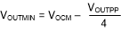
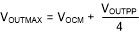
From target output VOCM, the next step is to verify that the desired output differential peak-to-peak voltage, VOUTPP, stays within the supplies. For any desired differential VOUTPP, make sure that the absolute maximum voltage at the output pins swings with Equation 1 and Equation 2, and confirm that these expressions are within the supply rails minus the output headroom required for the RRO device.
With the output headroom confirmed, the input junctions must also stay within the operating range. The input range limitations require a maximum 1.0-V headroom from the supply voltages (VS+ and VS–) over the full temperature range.