SBOSA00B December 2019 – August 2020 OPA1637
PRODUCTION DATA
- 1 Features
- 2 Applications
- 3 Description
- 4 Revision History
- 5 Pin Configuration and Functions
- 6 Specifications
- 7 Parameter Measurement Information
- 8 Detailed Description
- 9 Application and Implementation
- 10Power Supply Recommendations
- 11Layout
- 12Device and Documentation Support
- 13Mechanical, Packaging, and Orderable Information
Package Options
Mechanical Data (Package|Pins)
- DGK|8
Thermal pad, mechanical data (Package|Pins)
Orderable Information
9.1.1 Driving Capacitive Loads
The capacitive load of an ADC, or some other next-stage device, is commonly required to be driven. Directly connecting a capacitive load to the output pins of a closed-loop amplifier such as the OPA1637 can lead to an unstable response. One typical remedy to this instability is to add two small series resistors (RISO) at the outputs of the OPA1637 before the capacitive load. Good practice is to leave a place for the RISO elements in a board layout (a 0-Ω value initially) for later adjustment, in case the response appears unacceptable.
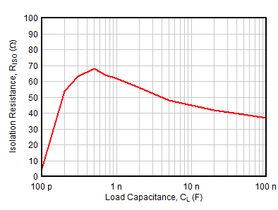
For applications where the OPA1637 is used as an output device to drive an unknown capacitive load, such as a cable, RISO is required. Figure 9-1 shows the required RISO value for a 40-degree phase-margin response. The peak required RISO value occurs when CL is between 500 pF and 1 nF. As CL increases beyond 1 nF, the bandwidth response of the device reduces, resulting in a slower response but no major degradation in phase margin. For a typical cable type, such as Belden 8451, capacitive loading can vary from 340 pF (10-foot cable) to 1.7 nF (50-foot cable). Selecting RISO to be 100 Ω provides sufficient phase margin regardless of the cable length. RISO can also be used within the loop feedback of the amplifier; however, simulation must be used to verify the stability of the system.
 Figure 9-1 Required Isolation Resistance vs Capacitive Load for a 40° Phase Margin