SBOS512E March   2010  – November 2020 OPA2365-Q1 , OPA365-Q1

PRODUCTION DATA  

  1. Features
  2. Applications
  3. Description
  4. Revision History
  5. Pin Configuration and Functions
  6. Specifications
    1. 6.1 Absolute Maximum Ratings
    2. 6.2 ESD Ratings
    3. 6.3 Recommended Operating Conditions
    4. 6.4 Thermal Information
    5. 6.5 Electrical Characteristics
    6. 6.6 Typical Characteristics
  7. Detailed Description
    1. 7.1 Overview
    2. 7.2 Functional Block Diagram
    3. 7.3 Feature Description
      1. 7.3.1 Operating Characteristics
      2. 7.3.2 Basic Amplifier Configurations
      3. 7.3.3 Input and ESD Protection
      4. 7.3.4 Rail-to-Rail Input
    4. 7.4 Device Functional Modes
  8. Application and Implementation
    1. 8.1 Application Information
      1. 8.1.1 Capacitive Loads
      2. 8.1.2 Achieving an Output Level of Zero Volts (0 V)
      3. 8.1.3 Active Filtering
      4. 8.1.4 Driving an ADS7822-Q1 Analog-to-Digital Converter
      5. 8.1.5 Driving ADS1115-Q1 Analog-to-Digital Converter
    2. 8.2 Typical Application
      1. 8.2.1 Fast Settling Peak Detector
        1. 8.2.1.1 Design Requirements
        2. 8.2.1.2 Detailed Design Procedure
        3. 8.2.1.3 Application Curves
      2. 8.2.2 Bandpass Filter 1.5 kHz to 160 kHz and 40-db Flat Gain
        1. 8.2.2.1 Design Requirements
        2. 8.2.2.2 Detailed Design Procedure
        3. 8.2.2.3 Application Curves
  9. Power Supply Recommendations
  10. 10Layout
    1. 10.1 Layout Guidelines
    2. 10.2 Layout Example
  11. 11Device and Documentation Support
    1. 11.1 Documentation Support
      1. 11.1.1 Related Documentation
    2. 11.2 Support Resources
    3. 11.3 Trademarks
    4. 11.4 Electrostatic Discharge Caution
    5. 11.5 Glossary
  12. 12Mechanical, Packaging, and Orderable Information

Package Options

Mechanical Data (Package|Pins)
Thermal pad, mechanical data (Package|Pins)
Orderable Information

Rail-to-Rail Input

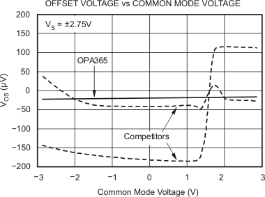
The OPA365-Q1 product family features true rail-to-rail input operation, with supply voltages as low as ±1.1 V (2.2 V). A unique zero-crossover input topology eliminates the input offset transition region typical of many rail-to-rail, complementary stage operational amplifiers. This topology also allows the OPA365-Q1 device to provide superior common-mode performance over the entire input range, which extends 100 mV beyond both power-supply rails, as shown in Figure 7-4. When driving ADCs, the highly linear VCM range of the OPA365-Q1 device assures that the operational amplifier/ADC system linearity performance is not compromised.
GUID-8E685FE0-649C-426A-B9CF-378FBBF99EBA-low.gifFigure 7-4 OPA365-Q1 Has Linear Offset Over the Entire Common-Mode Range