SBOS512E March 2010 – November 2020 OPA2365-Q1 , OPA365-Q1
PRODUCTION DATA
- 1 Features
- 2 Applications
- 3 Description
- 4 Revision History
- 5 Pin Configuration and Functions
- 6 Specifications
- 7 Detailed Description
- 8 Application and Implementation
- 9 Power Supply Recommendations
- 10Layout
- 11Device and Documentation Support
- 12Mechanical, Packaging, and Orderable Information
Package Options
Mechanical Data (Package|Pins)
- D|8
Thermal pad, mechanical data (Package|Pins)
Orderable Information
3 Description
The OPAx365-Q1 zero-crossover family, rail-to-rail, high-performance, CMOS operational amplifiers are optimized for very low voltage, single-supply applications. Rail-to-rail input/output, low noise (4.5 nV/√ Hz) and high speed operation (50-MHz gain bandwidth) make these devices ideal for driving sampling data converters (such as the ADS7822-Q1 or the ADS1115-Q1), specifically in short to mid-range radar applications. The OPAx356-Q1 family of operational amplifiers are also well-suited for HEV/EV and Powertrain applications in DC-DC converters and as transmission control in engine control units.
Special features include an excellent common-mode rejection ratio (CMRR), no input stage crossover distortion, high input impedance, and rail-to-rail input and output swing. The input common-mode range includes both the negative and positive supplies. The output voltage swing is within 10 mV of the rails.
The OPA365-Q1 (single version) is available in the 5-pin SOT-23 package. The OPA2365-Q1 (dual version) is available in the 8-pin SOIC package. All versions are specified for operation from −40°C to 125°C. Single and dual versions have identical specifications for maximum design flexibility.
| PART NUMBER | PACKAGE | BODY SIZE (NOM) |
|---|---|---|
| OPA2365-Q1 | SOIC (8) | 4.90 mm × 3.91 mm |
| OPA365-Q1 | SOT-23 (5) | 2.90 mm × 1.60 mm |
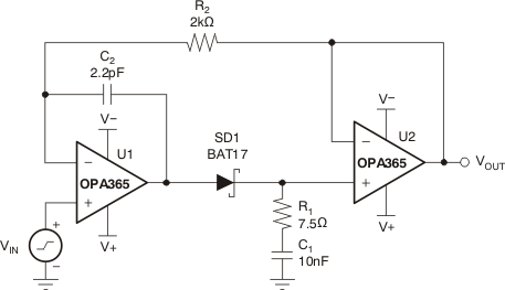
 Fast-Settling Peak Detector