SBOS981J October 2019 – April 2021 OPA2607 , OPA607
PRODUCTION DATA
- 1 Features
- 2 Applications
- 3 Description
- 4 Revision History
- 5 Device Comparison
- 6 Pin Configuration and Functions
- 7 Specifications
- 8 Detailed Description
- 9 Application and Implementation
- 10Power Supply Recommendations
- 11Layout
- 12Device and Documentation Support
- 13Mechanical, Packaging, and Orderable Information
Package Options
Mechanical Data (Package|Pins)
Thermal pad, mechanical data (Package|Pins)
Orderable Information
3 Description
The OPA607 and OPA2607 devices are decompensated, minimum gain of 6 V/V stable, general-purpose CMOS operational amplifier with low noise of 3.8 nV/√ Hz and a GBW of 50 MHz. The low noise and wide bandwidth of the OPAx607 devices make them attractive for general-purpose applications which require a good balance between cost and performance. The high-impedance CMOS inputs make the OPAx607 devices an ideal amplifier to interface with sensors with high output impedance (for example, piezoelectric transducers).
The OPAx607 devices feature a Power Down mode with a maximum quiescent current of less than 1 µA, making the device suitable for use in portable battery-powered applications. The rail-to-rail output (RRO) of the OPAx607 devices can swing up to 8 mV from the supply rails, maximizing dynamic range.
The OPAx607 is optimized for low supply voltage operation as low as 2.2 V (±1.1 V) and up to 5.5 V (±2.75 V), and is specified over the temperature range of –40°C to +125°C.
| PART NUMBER | PACKAGE | BODY SIZE (NOM) |
|---|---|---|
| OPA607 | SC70 (6) | 2.00 mm × 1.25 mm |
| SOT23 (5) | 2.90 mm × 1.60 mm | |
| OPA2607 | SOIC (8) | 4.90 mm × 3.91 mm |
| VSSOP (8) | 3.00 mm × 3.00 mm | |
| X2QFN (10) | 1.50 mm × 2.00 mm |
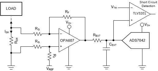
 OPAx607 for Current-Sensing
Application
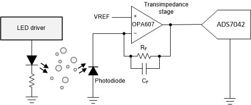
 OPAx607 for Transimpedance
Application