SBOS690A July 2016 – December 2019 OPA2626
PRODUCTION DATA.
- 1 Features
- 2 Applications
- 3 Description
- 4 Revision History
- 5 Pin Configuration and Functions
- 6 Specifications
- 7 Parameter Measurement Information
- 8 Detailed Description
- 9 Application and Implementation
- 10Power Supply Recommendations
- 11Layout
- 12Device and Documentation Support
- 13Mechanical, Packaging, and Orderable Information
Package Options
Mechanical Data (Package|Pins)
- DGK|8
Thermal pad, mechanical data (Package|Pins)
Orderable Information
8.3.2 Electrical Overstress
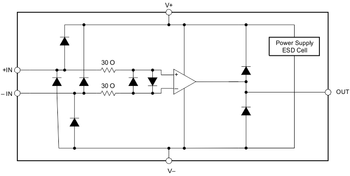
Designers often ask questions about the capability of an operational amplifier to withstand electrical overstress (EOS). These questions tend to focus on the device inputs, but may involve the supply voltage pins or even the output pin. Each of these different pin functions have electrical stress limits determined by the voltage breakdown characteristics of the particular semiconductor fabrication process and specific circuits connected to the pin. Additionally, internal electrostatic discharge (ESD) protection is built into these circuits to protect them from accidental ESD events both before and during product assembly. A good understanding of this basic ESD circuitry and how the ESD circuitry relates to an electrical overstress event is helpful. Figure 60 provides a diagram of the ESD circuits contained in the OPA2626. The ESD protection circuitry involves several current-steering diodes connected from the input and output pins and routed back to the internal power-supply lines, where the diodes meet at an absorption device or the power-supply ESD cell, internal to the operational amplifier. This protection circuitry is intended to remain inactive during normal circuit operation.
 Figure 60. Simplified ESD Circuit