SBOS382H may 2008 – june 2023 OPA2673
PRODUCTION DATA
- 1
- 1 Features
- 2 Applications
- 3 Description
- 4 Revision History
- 5 Device Family Comparison Table
- 6 Pin Configuration and Functions
-
7 Specifications
- 7.1 Absolute Maximum Ratings
- 7.2 ESD Ratings
- 7.3 Recommended Operating Conditions
- 7.4 Thermal Information
- 7.5 Electrical Characteristics: Full Bias and Offline Mode VS = ±6 V
- 7.6 Electrical Characteristics: 75% Bias Mode VS = ±6 V
- 7.7 Electrical Characteristics: 50% Bias Mode VS = ±6 V
- 7.8 Typical Characteristics: VS = ±6 V, Full Bias
- 7.9 Typical Characteristics: VS = ±6 V Differential, Full Bias
- 7.10 Typical Characteristics: VS = ±6 V, 75% Bias
- 7.11 Typical Characteristics: VS = ±6 V, 50% Bias
- 8 Detailed Description
- 9 Application and Implementation
- 10Device and Documentation Support
- 11Mechanical, Packaging, and Orderable Information
Package Options
Mechanical Data (Package|Pins)
- RGV|16
Thermal pad, mechanical data (Package|Pins)
- RGV|16
Orderable Information
8.3.1.5 Noise Performance
Wideband current-feedback op amps generally have a higher output noise than comparable voltage-feedback op amps. The OPA2673 offers an excellent balance between voltage and current noise terms to achieve low output noise. The low input voltage noise is achieved at the price of higher noninverting input current noise (3 pA/√ Hz). As long as the ac source impedance from the noninverting node is less than 100 Ω, this current noise does not contribute significantly to the total output noise. The op amp input voltage noise and the two input current noise terms combine to give low output noise under a wide variety of operating conditions. Figure 8-11 shows the op amp noise analysis model with all noise terms included. In this model, voltage noise and current noise have the units nV/√ Hz or pA/√ Hz.
 Figure 8-11 Op Amp Noise Analysis Model
The total output spot noise voltage can be computed as the square root of the sum of all squared output noise voltage contributors. Equation 11 shows the general form for the output noise voltage using the terms given in Figure 8-11.

Dividing this expression by the noise gain [NG = (1 + RF / RG)] gives the equivalent input-referred spot noise voltage at the noninverting input, as shown in Equation 12.
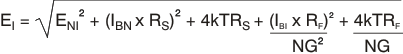
Evaluating these two equations for the OPA2673 circuit and component values of Figure 8-1 gives a total output spot noise voltage of 15.6 nV/√ Hz and a total equivalent input spot noise voltage of 3.9 nV/√ Hz. This total input-referred spot noise voltage is higher than the 2.4 nV/√ Hz specification for the op amp voltage noise alone. This result is due to the noise added to the output by the inverting current noise times the feedback resistor 402 Ω in this case. If the feedback resistor is reduced in high-gain configurations (as suggested previously), the total input-referred voltage noise given by Equation 12 approaches only the 2.4 nV/√ Hz of the op amp. For example, going to a gain of +8 V/V using RF = 250 Ω gives a total input-referred noise of 2.9 nV/√ Hz.