SBOS382H may 2008 – june 2023 OPA2673
PRODUCTION DATA
- 1
- 1 Features
- 2 Applications
- 3 Description
- 4 Revision History
- 5 Device Family Comparison Table
- 6 Pin Configuration and Functions
-
7 Specifications
- 7.1 Absolute Maximum Ratings
- 7.2 ESD Ratings
- 7.3 Recommended Operating Conditions
- 7.4 Thermal Information
- 7.5 Electrical Characteristics: Full Bias and Offline Mode VS = ±6 V
- 7.6 Electrical Characteristics: 75% Bias Mode VS = ±6 V
- 7.7 Electrical Characteristics: 50% Bias Mode VS = ±6 V
- 7.8 Typical Characteristics: VS = ±6 V, Full Bias
- 7.9 Typical Characteristics: VS = ±6 V Differential, Full Bias
- 7.10 Typical Characteristics: VS = ±6 V, 75% Bias
- 7.11 Typical Characteristics: VS = ±6 V, 50% Bias
- 8 Detailed Description
- 9 Application and Implementation
- 10Device and Documentation Support
- 11Mechanical, Packaging, and Orderable Information
Package Options
Mechanical Data (Package|Pins)
- RGV|16
Thermal pad, mechanical data (Package|Pins)
- RGV|16
Orderable Information
8.3 Feature Description
The OPA2673 gives exceptional ac performance with a highly linear, high-power output stage. Requiring 16‑mA/ch quiescent current, the OPA2673 swings to within 1.1 V of either supply rail and delivers in excess of 460 mA at room temperature. This low-output headroom requirement, along with supply voltage independent biasing, gives remarkable dual (±6 V) supply operation. The OPA2673 delivers greater than 450 MHz of bandwidth driving a 2-VPP output into 100 Ω on a single 12‑V supply.
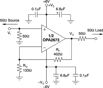
The primary advantage of a current-feedback op amp over a voltage-feedback op amp is that ac performance (bandwidth and distortion) is relatively independent of signal gain. Figure 8-1 shows the dc-coupled, gain of +4 V/V, dual power-supply circuit configuration used as the test circuit for the ±6‑V Electrical Characteristics and Typical Characteristics. Voltage swings reported in the Electrical Characteristics are taken directly at the input and output pins. For measuring the ac performance, the output of the OPA2673 is terminated with a matched 50‑Ω load. Thus, the total effective load seen by the OPA2673 is 100 Ω || 402 Ω = 80 Ω.
 Figure 8-1 DC-Coupled, G = +4 V/V,
Bipolar Supply