SBOS701D December 2015 – August 2021 OPA191 , OPA2191 , OPA4191
PRODUCTION DATA
- 1 Features
- 2 Applications
- 3 Description
- 4 Revision History
- 5 Pin Configuration and Functions
-
6 Specifications
- 6.1 Absolute Maximum Ratings
- 6.2 ESD Ratings
- 6.3 Recommended Operating Conditions
- 6.4 Thermal Information: OPA191
- 6.5 Thermal Information: OPA2191
- 6.6 Thermal Information: OPA4191
- 6.7 Electrical Characteristics: VS = ±4 V to ±18 V (VS = 8 V to 36 V)
- 6.8 Electrical Characteristics: VS = ±2.25 V to ±4 V (VS = 4.5 V to 8 V)
- 6.9 Typical Characteristics
- 7 Parameter Measurement Information
- 8 Detailed Description
- 9 Application and Implementation
- 10Power Supply Recommendations
- 11Layout
- 12Device and Documentation Support
- 13Mechanical, Packaging, and Orderable Information
Package Options
Mechanical Data (Package|Pins)
Thermal pad, mechanical data (Package|Pins)
- RUM|16
Orderable Information
8.3.5 Capacitive Load and Stability
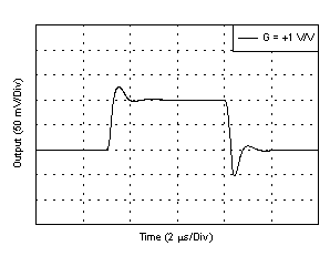
The OPAx191 features a patented output stage capable of driving large capacitive loads, and in a unity-gain configuration, directly drives up to 1 nF of pure capacitive load. Increasing the gain enhances the ability of the amplifier to drive greater capacitive loads; see Figure 8-5. The particular op amp circuit configuration, layout, gain, and output loading are some of the factors to consider when establishing whether an amplifier will be stable in operation.
 Figure 8-5 Transient Response with a Purely Capacitive Load of 1 nF
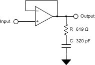
Like many low-power amplifiers, some ringing can occur even with capacitive loads less than 100 pF. In unity-gain configurations with no or very light dc loads, place an RC snubber circuit at the OPAx191 output to reduce any possibility of ringing in lightly-loaded applications. Figure 8-6 illustrates the recommended RC snubber circuit.
 Figure 8-6 RC Snubber Circuit for Lightly-Loaded Applications in Unity Gain
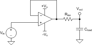
For additional drive capability in unity-gain configurations, improve capacitive load drive by inserting a small,
10-Ω to 20-Ω resistor (RISO) in series with the output, as shown in Figure 8-7. This resistor significantly reduces ringing while maintaining dc performance for purely capacitive loads. However, if there is a resistive load in parallel with the capacitive load, a voltage divider is created, introducing a gain error at the output and slightly reducing the output swing. The error introduced is proportional to the ratio RISO / RL, and is generally negligible at low output levels. A high capacitive load drive makes the OPA191 a great choice for applications such as reference buffers, MOSFET gate drives, and cable-shield drives. The circuit shown in Figure 8-7 uses RISO to stabilize the output of an op amp. RISO modifies the open-loop gain of the system for increased phase margin. Results using the OPA191 are summarized in Table 8-2. For additional information on techniques to optimize and design using this circuit, TI Precision Design TIPD128, Capacitive Load Drive Verified Reference Design Using an Isolation Resistor, details complete design goals, simulation, and test results.
 Figure 8-7 Extending Capacitive Load Drive With the OPA191
| PARAMETER | VALUE | ||||||||
|---|---|---|---|---|---|---|---|---|---|
| Capacitive Load | 100 pF | 1000 pF | 0.01 µF | 0.1 µF | 1 µF | ||||
| Phase Margin | 45° | 45° | 60° | 45° | 60° | 45° | 60° | 45° | 60° |
| RISO (Ω) | 280 | 113 | 432 | 68 | 210 | 17.8 | 53.6 | 3.6 | 10 |
| Measured Overshoot (%) | 23 | 23 | 8 | 23 | 8 | 23 | 8 | 23 | 8 |