SBOS701D December   2015  – August 2021 OPA191 , OPA2191 , OPA4191

PRODUCTION DATA  

  1. Features
  2. Applications
  3. Description
  4. Revision History
  5. Pin Configuration and Functions
  6. Specifications
    1. 6.1 Absolute Maximum Ratings
    2. 6.2 ESD Ratings
    3. 6.3 Recommended Operating Conditions
    4. 6.4 Thermal Information: OPA191
    5. 6.5 Thermal Information: OPA2191
    6. 6.6 Thermal Information: OPA4191
    7. 6.7 Electrical Characteristics: VS = ±4 V to ±18 V (VS = 8 V to 36 V)
    8. 6.8 Electrical Characteristics: VS = ±2.25 V to ±4 V (VS = 4.5 V to 8 V)
    9. 6.9 Typical Characteristics
  7. Parameter Measurement Information
    1. 7.1 Input Offset Voltage Drift
  8. Detailed Description
    1. 8.1 Overview
    2. 8.2 Functional Block Diagram
    3. 8.3 Feature Description
      1. 8.3.1 Input Protection Circuitry
      2. 8.3.2 EMI Rejection
      3. 8.3.3 Phase Reversal Protection
      4. 8.3.4 Thermal Protection
      5. 8.3.5 Capacitive Load and Stability
      6. 8.3.6 Common-Mode Voltage Range
      7. 8.3.7 Electrical Overstress
      8. 8.3.8 Overload Recovery
    4. 8.4 Device Functional Modes
  9. Application and Implementation
    1. 9.1 Application Information
    2. 9.2 Typical Applications
      1. 9.2.1 Low-side Current Measurement
        1. 9.2.1.1 Design Requirements
        2. 9.2.1.2 Detailed Design Procedure
        3. 9.2.1.3 Application Curves
      2. 9.2.2 16-Bit Precision Multiplexed Data-Acquisition System
        1. 9.2.2.1 Design Requirements
        2. 9.2.2.2 Detailed Design Procedure
      3. 9.2.3 Slew Rate Limit for Input Protection
  10. 10Power Supply Recommendations
  11. 11Layout
    1. 11.1 Layout Guidelines
    2. 11.2 Layout Example
  12. 12Device and Documentation Support
    1. 12.1 Device Support
      1. 12.1.1 Development Support
        1. 12.1.1.1 TINA-TI™ SImulation Software (Free Download)
        2. 12.1.1.2 TI Precision Designs
    2. 12.2 Documentation Support
      1. 12.2.1 Related Documentation
    3. 12.3 Receiving Notification of Documentation Updates
    4. 12.4 Support Resources
    5. 12.5 Trademarks
    6. 12.6 Electrostatic Discharge Caution
    7. 12.7 Glossary
  13. 13Mechanical, Packaging, and Orderable Information

Package Options

Mechanical Data (Package|Pins)
Thermal pad, mechanical data (Package|Pins)
Orderable Information

Low-side Current Measurement

Figure 9-1 shows the OPA191 configured in a low-side current sensing application. For a full analysis of the circuit shown in Figure 9-1 including theory, calculations, simulations, and measured data, see TI Precision Design TIPD129, 0-A to 1-A Single-Supply Low-Side Current-Sensing Solution .
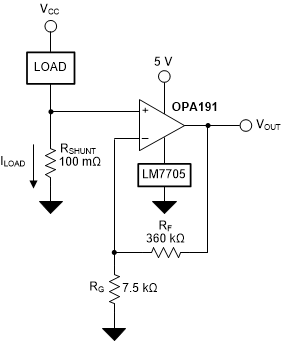
GUID-61CDBCD6-2120-42BF-A7E4-433F6455C895-low.gifFigure 9-1 OPA191 in a Low-Side, Current-Sensing Application