SBOS933I February 2019 – August 2021 OPA2990 , OPA4990 , OPA990
PRODUCTION DATA
- 1 Features
- 2 Applications
- 3 Description
- 4 Revision History
- 5 Pin Configuration and Functions
- 6 Specifications
-
7 Detailed Description
- 7.1 Overview
- 7.2 Functional Block Diagram
- 7.3
Feature Description
- 7.3.1 Input Protection Circuitry
- 7.3.2 EMI Rejection
- 7.3.3 Thermal Protection
- 7.3.4 Capacitive Load and Stability
- 7.3.5 Common-Mode Voltage Range
- 7.3.6 Phase Reversal Protection
- 7.3.7 Electrical Overstress
- 7.3.8 Overload Recovery
- 7.3.9 Typical Specifications and Distributions
- 7.3.10 Packages With an Exposed Thermal Pad
- 7.3.11 Shutdown
- 7.4 Device Functional Modes
- 8 Application and Implementation
- 9 Power Supply Recommendations
- 10Layout
- 11Device and Documentation Support
- 12Mechanical, Packaging, and Orderable Information
Package Options
Mechanical Data (Package|Pins)
Thermal pad, mechanical data (Package|Pins)
Orderable Information
7.3.5 Common-Mode Voltage Range
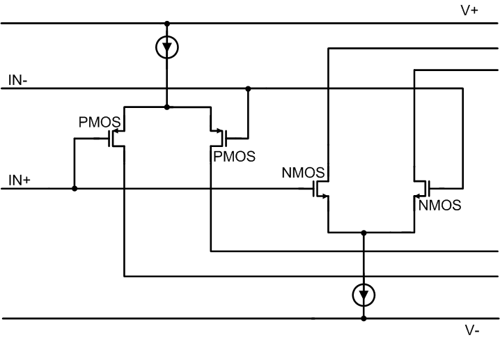
The OPAx990 is a 40-V, true rail-to-rail input operational amplifier with an input common-mode range that extends 200 mV beyond either supply rail. This wide range is achieved with paralleled complementary N-channel and P-channel differential input pairs, as shown in Figure 7-8. The N-channel pair is active for input voltages close to the positive rail, typically (V+) – 1 V to 100 mV above the positive supply. The P-channel pair is active for inputs from 100 mV below the negative supply to approximately (V+) – 2 V. There is a small transition region, typically (V+) – 2 V to (V+) – 1 V in which both input pairs are on. This transition region can vary modestly with process variation, and within this region PSRR, CMRR, offset voltage, offset drift, noise, and THD performance may be degraded compared to operation outside this region.
Figure 6-5 shows this transition region for a typical device in terms of input voltage offset in more detail.
For more information on common-mode voltage range and PMOS/NMOS pair interaction, see Op Amps With Complementary-Pair Input Stages application note.
 Figure 7-8 Rail-to-Rail Input Stage