SCPS124H September   2006  – March 2021 PCA9534

PRODUCTION DATA  

  1. Features
  2. Description
  3. Revision History
  4. Description (Continued)
  5. Device Comparison Table
  6. Pin Configuration and Functions
  7. Specifications
    1. 7.1 Absolute Maximum Ratings
    2. 7.2 ESD Ratings
    3. 7.3 Recommended Operating Conditions
    4. 7.4 Thermal Resistance Characteristics
    5. 7.5 Electrical Characteristics
    6. 7.6 I2C Interface Timing Requirements
    7. 7.7 Switching Characteristics
    8. 7.8 Typical Characteristics
  8. Parameter Measurement Information
  9. Detailed Description
    1. 9.1 Functional Block Diagram
    2. 9.2 Device Functional Modes
      1. 9.2.1 Power-On Reset
      2. 9.2.2 I/O Port
      3. 9.2.3 Interrupt Output ( INT)
        1. 9.2.3.1 Interrupt Errata
          1. 9.2.3.1.1 Description
          2. 9.2.3.1.2 System Impact
          3. 9.2.3.1.3 System Workaround
    3. 9.3 Programming
      1. 9.3.1 I2C Interface
      2. 9.3.2 Register Map
        1. 9.3.2.1 Device Address
        2. 9.3.2.2 Control Register And Command Byte
        3. 9.3.2.3 Register Descriptions
        4. 9.3.2.4 Bus Transactions
          1. 9.3.2.4.1 Writes
          2. 9.3.2.4.2 Reads
  10. 10Application Information Disclaimer
    1. 10.1 Application Information
      1. 10.1.1 Typical Application
        1. 10.1.1.1 Design Requirements
          1. 10.1.1.1.1 Minimizing ICC When The I/O Controls Leds
  11. 11Power Supply Recommendations
    1. 11.1 Power-On Reset Requirements
  12. 12Device and Documentation Support
    1. 12.1 Receiving Notification of Documentation Updates
    2. 12.2 Support Resources
    3. 12.3 Trademarks
    4. 12.4 Electrostatic Discharge Caution
    5. 12.5 Glossary
  13. 13Mechanical, Packaging, and Orderable Information

Package Options

Mechanical Data (Package|Pins)
Thermal pad, mechanical data (Package|Pins)
Orderable Information
Reads

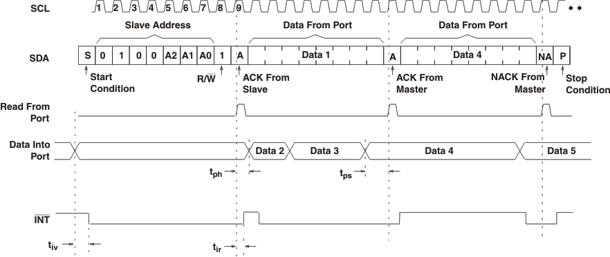
The bus master first must send the PCA9534 address with the LSB set to a logic 0 (see Figure 9-6 for device address). The command byte is sent after the address and determines which register is accessed. After a restart, the device address is sent again but, this time, the LSB is set to a logic 1. Data from the register defined by the command byte then is sent by the PCA9534 (see Figure 9-10 and Figure 9-11). After a restart, the value of the register defined by the command byte matches the register being accessed when the restart occurred. Data is clocked into the register on the rising edge of the ACK clock pulse. There is no limitation on the number of data bytes received in one read transmission, but when the final byte is received, the bus master must not acknowledge the data.

GUID-D69778C1-41A9-4ED2-9AF3-C2D7D53FFACF-low.gifFigure 9-10 Read From Register

GUID-AEDA05DA-E10D-4346-A939-3E85FD8AA920-low.gif
This figure assumes that the command byte has previously been programmed with 00h.
Transfer of data can be stopped at any moment by a Stop condition.
This figure eliminates the command byte transfer, a restart and slave address call between the initial slave address call and the actual data transfer from the P Port. See Figure 9-10 for these details.
Figure 9-11 Read Input Port Register