SBOS600E July 2018 – February 2022 REF2025 , REF2030 , REF2033 , REF2041
PRODUCTION DATA
- 1 Features
- 2 Applications
- 3 Description
- 4 Revision History
- 5 Device Comparison Table
- 6 Pin Configuration and Functions
- 7 Specifications
- 8 Parameter Measurement Information
- 9 Detailed Description
- 10Applications and Implementation
- 11Power-Supply Recommendations
- 12Layout
- 13Device and Documentation Support
- 14Mechanical, Packaging, and Orderable Information
Package Options
Mechanical Data (Package|Pins)
- DDC|5
Thermal pad, mechanical data (Package|Pins)
Orderable Information
10.2.1.2.3 Voltage Reference
The voltage reference for this application should have the following features:
- Dual output (3.0 V and 1.5 V),
- Low drift, and
- Low tracking errors between the two outputs.
For this design, the REF2030 is used. The REF20xx topology is as shown in the Section 9.2 section.
The REF2030 is an excellent choice for this application because of its dual output. The temperature drift of
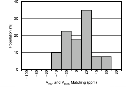
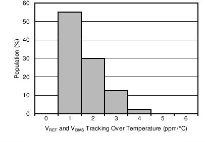
8 ppm/°C and initial accuracy of 0.05% make the errors resulting from the voltage reference minimal in this application. In addition, there is minimal mismatch between the two outputs and both outputs track very well across temperature, as shown in Figure 10-4 and Figure 10-5.
 Figure 10-4 VREF – 2 × VBIAS Distribution (At TA = 25°C)
 Figure 10-5 Distribution of VREF – 2 × VBIAS Drift Tracking Over Temperature