SBOS600E July 2018 – February 2022 REF2025 , REF2030 , REF2033 , REF2041
PRODUCTION DATA
- 1 Features
- 2 Applications
- 3 Description
- 4 Revision History
- 5 Device Comparison Table
- 6 Pin Configuration and Functions
- 7 Specifications
- 8 Parameter Measurement Information
- 9 Detailed Description
- 10Applications and Implementation
- 11Power-Supply Recommendations
- 12Layout
- 13Device and Documentation Support
- 14Mechanical, Packaging, and Orderable Information
Package Options
Mechanical Data (Package|Pins)
- DDC|5
Thermal pad, mechanical data (Package|Pins)
Orderable Information
10.2.1.2 Detailed Design Procedure
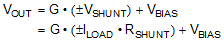
Low-side current sensing is desirable because the common-mode voltage is near ground. Therefore, the current-sensing solution is independent of the bus voltage, VBUS. When sensing bidirectional currents, use a differential amplifier with a reference pin. This procedure allows for the differentiation between positive and negative currents by biasing the output stage such that it can respond to negative input voltages. There are a variety of methods for supplying power (V+) and the reference voltage (VREF, or VBIAS) to the differential amplifier. For a low-drift solution, use a monolithic reference that supplies both power and the reference voltage. Figure 10-2 shows the general circuit topology for a low-drift, low-side, bidirectional, current-sensing solution. This topology is particularly useful when interfacing with an ADC; see Figure 10-1. Not only do VREF and VBIAS track over temperature, but their matching is much better than alternate topologies. For a more detailed version of the design procedure, refer to TIDU357.
 Figure 10-2 Low-Drift, Low-side, Bidirectional, Current-Sensing Circuit Topology
The transfer function for the circuit given in Figure 10-2 is as shown in Equation 5: