SBAS901C July 2018 – October 2020 REF34-Q1
PRODUCTION DATA
- 1 Features
- 2 Applications
- 3 Description
- 4 Revision History
- 5 Device Comparison Table
- 6 Pin Configuration and Functions
- 7 Specifications
- 8 Typical Characteristics
- 9 Parameter Measurement Information
- 10Detailed Description
- 11Application and Implementation
- 12Power Supply Recommendations
- 13Layout
- 14Device and Documentation Support
- 15Mechanical, Packaging, and Orderable Information
Package Options
Mechanical Data (Package|Pins)
Thermal pad, mechanical data (Package|Pins)
- DGK|8
Orderable Information
9.3 Thermal Hysteresis
Thermal hysteresis is measured with the REF34-Q1 soldered to a PCB, similar to a real-world application. Thermal hysteresis for the device is defined as the change in output voltage after operating the device at 25°C, cycling the device through the specified temperature range, and returning to 25°C. Hysteresis can be expressed by Equation 1:
Equation 1. 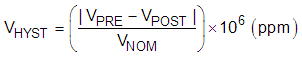
where
- VHYST = thermal hysteresis (in units of ppm)
- VNOM = the specified output voltage
- VPRE = output voltage measured at 25°C pre-temperature cycling
- VPOST = output voltage measured after the device has cycled from 25°C through the specified temperature range of –40°C to +125°C and returns to 25°C.
Typical thermal hysteresis distribution is as shown in Figure 9-6.
 - DBV Package (Cycle
1)") Figure 9-6 Thermal Hysteresis Distribution (VREF) - DBV Package (Cycle
1)
Figure 9-6 Thermal Hysteresis Distribution (VREF) - DBV Package (Cycle
1) - DGK Package (Cycle
1)") Figure 9-8 Thermal Hysteresis Distribution (VREF) - DGK Package (Cycle
1)
Figure 9-8 Thermal Hysteresis Distribution (VREF) - DGK Package (Cycle
1) - DBV Package (Cycle 2)") Figure 9-7 Thermal Hysteresis
Distribution (VREF) - DBV Package (Cycle 2)
Figure 9-7 Thermal Hysteresis
Distribution (VREF) - DBV Package (Cycle 2) - DGK Package (Cycle
2)") Figure 9-9 Thermal Hysteresis Distribution (VREF) - DGK Package (Cycle
2)
Figure 9-9 Thermal Hysteresis Distribution (VREF) - DGK Package (Cycle
2)