SBAS221H December 2001 – October 2015 REG71050 , REG71055
PRODUCTION DATA.
- 1 Features
- 2 Applications
- 3 Description
- 4 Revision History
- 5 Device Comparison Table
- 6 Pin Configuration and Functions
- 7 Specifications
- 8 Detailed Description
- 9 Application and Implementation
- 10Power Supply Recommendations
- 11Layout
- 12Device and Documentation Support
- 13Mechanical, Packaging, and Orderable Information
Package Options
Mechanical Data (Package|Pins)
Thermal pad, mechanical data (Package|Pins)
- DRV|6
Orderable Information
9 Application and Implementation
NOTE
Information in the following applications sections is not part of the TI component specification, and TI does not warrant its accuracy or completeness. TI’s customers are responsible for determining suitability of components for their purposes. Customers should validate and test their design implementation to confirm system functionality.
9.1 Application Information
The REG710 is a switched capacitor voltage converter that produces a regulated, low-ripple output voltage from an unregulated input voltage range from 1.8 V to 5.5 V. The high switching frequency allows the use of small surface-mount capacitors. The following section gives guidance to choose external components to complete the power supply design. Application curves are included for the typical application shown below.
9.2 Typical Applications
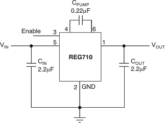 Figure 7. Typical Operating Circuit
9.2.1 Design Requirements
The REG710 family of switched capacitor voltage converters offers a variety of regulated fixed output voltages. This family supports unregulated input voltages which can have values that are lower or higher than the regulated output voltage. Only input and output capacitors as well as a pump capacitor are required to have a fully functional converter. The following design procedure is adequate for the whole VIN, VOUT and load current range of REG710.
9.2.2 Detailed Design Procedure
9.2.2.1 Capacitor Selection
For minimum output voltage ripple, the output capacitor COUT should be a ceramic, surface-mount type. Tantalum capacitors generally have a higher effective series resistance (ESR) and may contribute to higher output voltage ripple. Leaded capacitors also increase ripple due to the higher inductance of the package itself. To achieve best operation with low input voltage and high load current, the input and pump capacitors (CIN and CPUMP, respectively) should also be surface-mount ceramic types. In all cases, X7R or X5R dielectric are recommended. See the typical operating circuit shown in Figure 7 for component values.
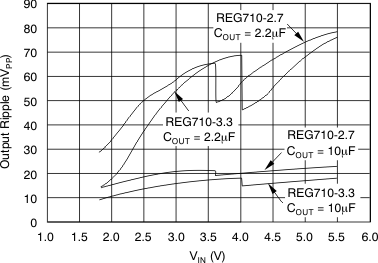
With light loads or higher input voltage, a smaller 0.1-μF pump capacitor (CPUMP) and smaller 1-μF input and output capacitors (CIN and COUT, respectively) can be used. To minimize output voltage ripple, increase the output capacitor, COUT, to 10 μF or larger.
The capacitors listed in Table 2 can be used with the REG710. This table is only a representative list of compatible parts.
Table 2. Suggested Capacitors
| MANUFACTURER | PART NUMBER | VALUE | TOLERANCE | DIELECTRIC MATERIAL | PACKAGE SIZE | RATED WORKING VOLTAGE |
|---|---|---|---|---|---|---|
| Kemet | C1206C255K8RAC | 2.2 μF | ±10% | X7R | 1206 | 10 V |
| C1206C224K8RAC | 0.22 μF | ±10% | X7R | 1206 | 10 V | |
| Panasonic | ECJ−2YBOJ225K | 2.2 μF | ±10% | X5R | 805 | 6.3 V |
| ECJ−2VBIC224K | 0.22 μF | ±10% | X7R | 805 | 16 V | |
| ECJ−2VBIC104 | 0.1 μF | ±10% | X7R | 805 | 16 V | |
| Taiyo Yuden | EMK316BJ225KL | 2.2 μF | ±10% | X7R | 1206 | 16 V |
| TKM316BJ224KF | 0.22 μF | ±10% | X7R | 1206 | 25 V |
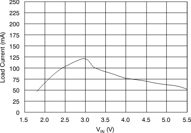
9.2.3 Application Curves
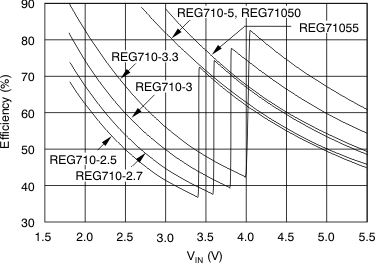
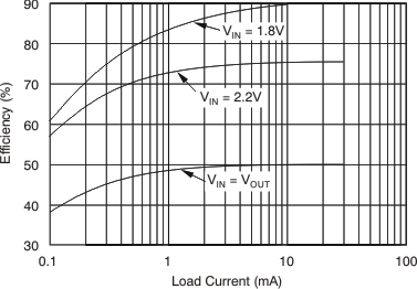
| REG710-3.3V | ||
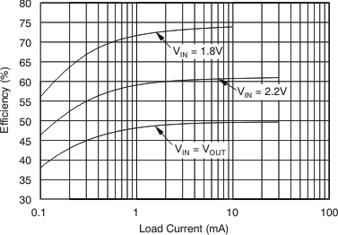
| REG710-2.7V | ||
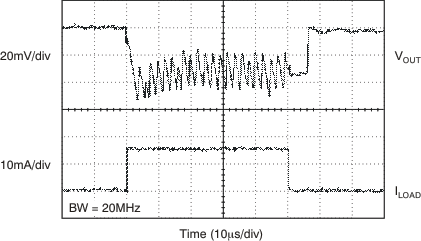
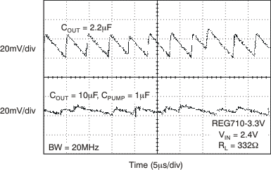
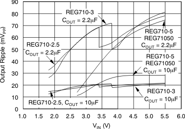
| REG710-2.5 | REG710-5 | |
| REG710-3 |
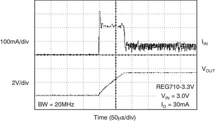
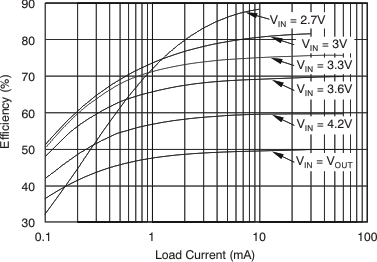
| REG710-5V, REG71050 | ||
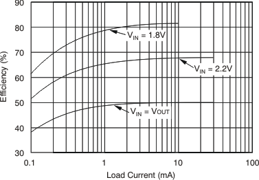
| REG710-3.3V | ||
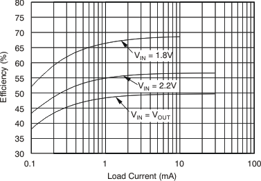
| REG710-2.5 | ||
| REG710-2.7V | ||
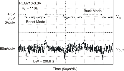
| REG710-3.3V |
9.3 System Examples
9.3.1 1.8 V to 5.0 V With 10-mA Output Current
The REG710 family of charge pumps can be cascaded to reach higher output voltages, as shown in Figure 21.
 Figure 21. REG710 Circuit for Step-Up Operation From 1.8 V to 5 V With 10-mA Output Current
This application circuits operates from 1.8 V input voltage and generates 5 V output voltage supporting 10 mA load current.
Higher output voltages can be achieved when two REG710 devices are connected in cascade. When cascading two devices from the REG710 family, the relationship between output current and input voltage must be taken into account. (see Electrical Characteristics). In this case, REG710 can deliver a maximum of 10 mA. REG710-3.3 or REG710-3 can be used. A second charge pump, REG71050 or REG710-5, steps up the voltage from 3 V or 3.3 V to 5 V. Connect both Enable pins together.
9.3.2 Doubling the Output Current
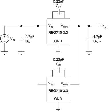 Figure 22. REG710 Circuit for Doubling the Output Current
When higher output currents are required, the REG710 family can be paralleled to double the output current. When paralleling two devices the relationship between output current and input voltage must be taken into account (see Electrical Characteristics).
This particular application can deliver 20 mA for an input voltage from 1.8 V to 5.5 V, or 60-mA output for an input voltage from 2.2 V to 5.5 V. The output voltage is 3.3 V.
9.3.3 Driving LEDs
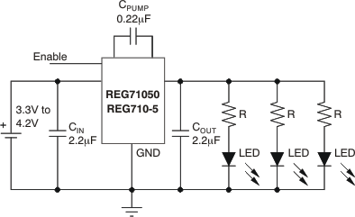 Figure 23. REG710 Circuit for Driving LEDs
The REG710 family can be used to drive LEDs. The feed forward voltage of the chosen LED determines the required output voltage. In this application, the charge pump can drive multiple LEDs up to 60 mA in total.
