SBAS221H December   2001  – October  2015 REG71050 , REG71055

PRODUCTION DATA.  

  1. Features
  2. Applications
  3. Description
  4. Revision History
  5. Device Comparison Table
  6. Pin Configuration and Functions
  7. Specifications
    1. 7.1 Absolute Maximum Ratings
    2. 7.2 ESD Ratings
    3. 7.3 Recommended Operating Conditions
    4. 7.4 Thermal Information
    5. 7.5 Electrical Characteristics
    6. 7.6 Typical Characteristics
  8. Detailed Description
    1. 8.1 Overview
    2. 8.2 Functional Block Diagram
    3. 8.3 Feature Description
      1. 8.3.1 Shutdown Mode
      2. 8.3.2 Protection
    4. 8.4 Device Functional Modes
      1. 8.4.1 Peak Current Reduction
      2. 8.4.2 Efficiency
  9. Application and Implementation
    1. 9.1 Application Information
    2. 9.2 Typical Applications
      1. 9.2.1 Design Requirements
      2. 9.2.2 Detailed Design Procedure
        1. 9.2.2.1 Capacitor Selection
      3. 9.2.3 Application Curves
    3. 9.3 System Examples
      1. 9.3.1 1.8 V to 5.0 V With 10-mA Output Current
      2. 9.3.2 Doubling the Output Current
      3. 9.3.3 Driving LEDs
  10. 10Power Supply Recommendations
  11. 11Layout
    1. 11.1 Layout Guidelines
    2. 11.2 Layout Example
  12. 12Device and Documentation Support
    1. 12.1 Device Support
      1. 12.1.1 Third-Party Products Disclaimer
    2. 12.2 Related Links
    3. 12.3 Community Resources
    4. 12.4 Trademarks
    5. 12.5 Electrostatic Discharge Caution
    6. 12.6 Glossary
  13. 13Mechanical, Packaging, and Orderable Information

Package Options

Mechanical Data (Package|Pins)
Thermal pad, mechanical data (Package|Pins)
Orderable Information

11 Layout

11.1 Layout Guidelines

Large transient currents flow in the VIN, VOUT, and GND traces. To minimize both input and output ripple, keep the capacitors as close as possible to the regulator using short, direct circuit traces.

A suggested printed-circuit-board (PCB) routing is shown in Figure 24. The trace lengths from the input and output capacitors have been kept as short as possible.

11.2 Layout Example
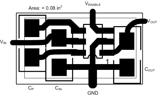
REG71050 REG71055 REG710 ai_pcb_ripple_bas221.gif Figure 24. Suggested PCB Design for Minimum Ripple