SBAS221H December 2001 – October 2015 REG71050 , REG71055
PRODUCTION DATA.
- 1 Features
- 2 Applications
- 3 Description
- 4 Revision History
- 5 Device Comparison Table
- 6 Pin Configuration and Functions
- 7 Specifications
- 8 Detailed Description
- 9 Application and Implementation
- 10Power Supply Recommendations
- 11Layout
- 12Device and Documentation Support
- 13Mechanical, Packaging, and Orderable Information
Package Options
Mechanical Data (Package|Pins)
Thermal pad, mechanical data (Package|Pins)
- DRV|6
Orderable Information
6 Pin Configuration and Functions
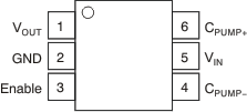
DDC and DBV Package
6-Pin SOT and SOT-23
Top View

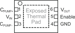
DRV Package
6-Pin SON With Exposed Thermal Pad
Top View

Pin Functions
| PIN | I/O | DESCRIPTION | ||
|---|---|---|---|---|
| NAME | DDC/DBV | DRV | ||
| Cpump- | 4 | 3 | – | Connect to the flying capacitor |
| Cpump+ | 6 | 1 | – | Connect to the flying capacitor |
| Enable | 3 | 5 | I | Hardware Enable/Disable pin (high=enable) |
| GND | 2 | 4 | – | Ground |
| Vin | 5 | 2 | I | Input supply pin. Connect the input capacitor to this pin. |
| Vout | 1 | 6 | O | Output supply. Connect the output capacitor to this pin. |