SLLSF98 December 2018 SN55HVD233-SEP
PRODUCTION DATA.
- 1 Features
- 2 Applications
- 3 Description
- 4 Revision History
- 5 Description (continued)
- 6 Pin Configuration and Functions
-
7 Specifications
- 7.1 Absolute Maximum Ratings
- 7.2 ESD Ratings
- 7.3 Recommended Operating Conditions
- 7.4 Thermal Information
- 7.5 Driver Electrical Characteristics
- 7.6 Receiver Electrical Characteristics
- 7.7 Driver Switching Characteristics
- 7.8 Receiver Switching Characteristics
- 7.9 Device Switching Characteristics
- 7.10 Typical Characteristics
- 8 Parameter Measurement Information
- 9 Detailed Description
- 10Application and Implementation
- 11Power Supply Recommendations
- 12Layout
- 13Device and Documentation Support
- 14Mechanical, Packaging, and Orderable Information
Package Options
Mechanical Data (Package|Pins)
- D|8
Thermal pad, mechanical data (Package|Pins)
Orderable Information
9.3.4.2 Differential Signal
CAN is a differential bus where complementary signals are sent over two wires and the voltage difference between the two wires defines the logical state of the bus. The differential CAN receiver monitors this voltage difference and outputs the bus state with a single-ended output signal.
 Figure 27. Typical SN55HVD233-SEP Differential Output Voltage Waveform
 The CAN driver creates the difference in voltage between CANH and CANL in the dominant state. The dominant differential output of the SN55HVD233-SEP is greater than 1.5 V and less than 3 V across a 60-Ω load. The minimum required by ISO 11898 is 1.5 V and maximum is 3 V. These are the same limiting values for 5-V supplied CAN transceivers. The bus termination resistors drive the recessive bus state and not the CAN driver.
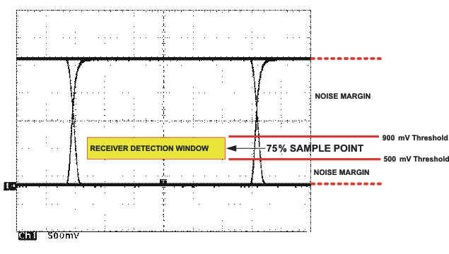
A CAN receiver is required to output a recessive state with less than 500 mV and a dominant state with more than 900-mV difference voltage on its bus inputs. The CAN receiver must do this with common-mode input voltages from –2 V to 7 V. The SN55HVD233-SEP receiver meets these same input specifications as 5-V supplied receivers.