SLLSFM0A March   2022  – June 2022 SN6507

PRODUCTION DATA  

  1. Features
  2. Applications
  3. Description
  4. Revision History
  5. Pin Configuration and Functions
  6. Specifications
    1. 6.1 Absolute Maximum Ratings
    2. 6.2 ESD Ratings
    3. 6.3 Recommended Operating Conditions
    4. 6.4 Thermal Information
    5. 6.5 Electrical Characteristics
    6. 6.6 Switching Characteristics
    7. 6.7 Typical Characteristics, SN6507
  7. Parameter Measurement Information
  8. Detailed Description
    1. 8.1 Overview
    2. 8.2 Functional Block Diagram
    3. 8.3 Feature Description
      1. 8.3.1 Push-Pull Converter
      2. 8.3.2 Core Magnetization
      3. 8.3.3 Duty Cycle Control
      4.      Programmable Switching Frequency
      5. 8.3.4 Spread Spectrum Clocking
      6. 8.3.5 Slew Rate Control
      7. 8.3.6 Protection Features
        1. 8.3.6.1 Over Voltage Protection (OVP)
        2. 8.3.6.2 Over Current and Short Circuit Protection (OCP)
        3. 8.3.6.3 Under Voltage Lock-Out (UVLO)
        4. 8.3.6.4 Thermal Shut Down (TSD)
    4. 8.4 Device Functional Modes
      1. 8.4.1 Start-Up Mode
        1. 8.4.1.1 Soft-Start
      2. 8.4.2 Operation Mode
      3. 8.4.3 Shutdown Mode
      4. 8.4.4 SYNC Mode
  9. Application and Implementation
    1. 9.1 Application Information
    2. 9.2 Typical Application
      1. 9.2.1 Design Requirements
      2. 9.2.2 Detailed Design Procedure
        1. 9.2.2.1 Pin Configuration
        2. 9.2.2.2 LDO Selection
        3. 9.2.2.3 Diode Selection
        4. 9.2.2.4 Capacitor and Inductor Selection
        5. 9.2.2.5 Transformer Selection
          1. 9.2.2.5.1 V-t Product Calculation
          2. 9.2.2.5.2 Turns Ratio Estimate
        6. 9.2.2.6 Low-Emissions Designs
      3. 9.2.3 Application Curves
      4. 9.2.4 System Examples
        1. 9.2.4.1 Higher Output Voltage Designs
        2. 9.2.4.2 Commercially-Available Transformers
    3. 9.3 Power Supply Recommendations
    4. 9.4 Layout
      1. 9.4.1 Layout Guidelines
      2. 9.4.2 Layout Example
  10. 10Device and Documentation Support
    1. 10.1 Documentation Support
      1. 10.1.1 Related Documentation
    2. 10.2 Receiving Notification of Documentation Updates
    3. 10.3 Community Resources
    4. 10.4 Trademarks
  11. 11Mechanical, Packaging, and Orderable Information

Package Options

Mechanical Data (Package|Pins)
Thermal pad, mechanical data (Package|Pins)
Orderable Information

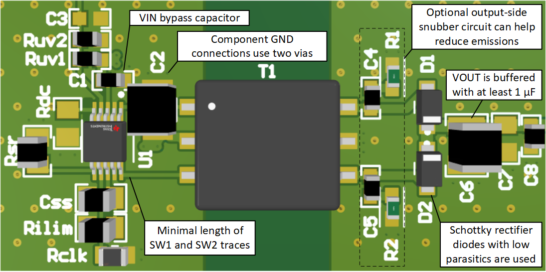
Layout Example

GUID-38F20C6B-5F5D-46C2-BC98-1C51BE922971-low.pngFigure 9-10 Layout Example of a 2-Layer Board