SLLS631E April 2007 – August 2015 SN65HVD1040
PRODUCTION DATA.
- 1 Features
- 2 Applications
- 3 Description
- 4 Revision History
- 5 Description (continued)
- 6 Pin Configuration and Functions
-
7 Specifications
- 7.1 Absolute Maximum Ratings
- 7.2 ESD Ratings
- 7.3 Recommended Operating Conditions
- 7.4 Thermal Information
- 7.5 Driver Electrical Characteristics
- 7.6 Receiver Electrical Characteristics
- 7.7 Device Switching Characteristics
- 7.8 Driver Switching Characteristics
- 7.9 Receiver Switching Characteristics
- 7.10 Dissipation Ratings
- 7.11 Supply Current
- 7.12 Split-Pin Characteristics
- 7.13 STB-Pin Characteristics
- 7.14 Typical Characteristics
- 8 Parameter Measurement Information
- 9 Detailed Description
- 10Application and Implementation
- 11Power Supply Recommendations
- 12Layout
- 13Device and Documentation Support
- 14Mechanical, Packaging, and Orderable Information
Package Options
Mechanical Data (Package|Pins)
- D|8
Thermal pad, mechanical data (Package|Pins)
Orderable Information
8 Parameter Measurement Information
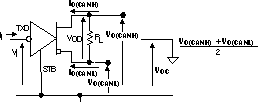
 Figure 11. Driver Voltage, Current, and Test Definition
 Figure 12. Bus Logic State Voltage Definitions
 Figure 13. Driver VOD Test Circuit
 Figure 14. Driver Test Circuit and Voltage Waveforms
 Figure 15. Receiver Voltage and Current Definitions

A. The input pulse is supplied by a generator having the following characteristics: PRR ≤ 125 kHz, 50% duty cycle, tr ≤ 6 ns, tf ≤ 6ns, ZO = 50 Ω.
B. CL includes instrumentation and fixture capacitance within ±20%.
Figure 16. Receiver Test Circuit and Voltage Waveforms
Table 1. Differential Input Voltage Threshold Test
 Figure 17. Ten Test Circuit and Voltage Waveforms

All VI input pulses are from 0 V to VCC and supplied by a generator having the following characteristics: tr or tf ≤ 6 ns. Pulse Repetition Rate (PRR) = 125 kHz, 50% duty cycle.
Figure 18. Peak-To-Peak Common Mode Output Voltage Test and Waveform

All VI input pulses are from 0 V to VCC and supplied by a generator with the following characteristics: tr or tf ≤ 6 ns. Pulse Repetition Rate (PRR) = 125 kHz, 50% duty cycle.
Figure 19. Tloop Test Circuit and Voltage Waveforms

All VI input pulses are from 0 V to VCC and supplied by a generator with the following characteristics: tr or tf ≤ 6 ns. Pulse Repetition Rate (PRR) = 500 Hz, 50% duty cycle.
A. CL = 100 pF includes instrumentation and fixture capacitance within ±20%.
Figure 20. Dominant Time-Out Test Circuit and Waveform

A. For VI bit width ≤ 0.7 μs, VO = VOH. For VII bit width ≥ 5 μs, VO = VOL. VI input pulses are supplied from a generator with the following characteristics; tr or tf ≤ 6 ns. Pulse Repetition Rate (PRR) = 50 Hz, 30% duty cycle.
B. CL = 15 pF includes instrumentation and fixture capacitance within ±20%.
Figure 21. TBUS Test Circuit and Waveform
 Figure 22. Driver Short-Circuit Current Test and Waveform
 Figure 23. Driver Output Symmetry Test Circuit