SLLSEA2D December 2011 – May 2015 SN65HVD255 , SN65HVD256 , SN65HVD257
PRODUCTION DATA.
- 1 Features
- 2 Applications
- 3 Description
- 4 Revision History
- 5 Device Options
- 6 Pin Configuration and Functions
- 7 Specifications
- 8 Parameter Measurement Information
- 9 Detailed Description
- 10Application and Implementation
- 11Power Supply Recommendations
- 12Layout
- 13Device and Documentation Support
- 14Mechanical, Packaging, and Orderable Information
Package Options
Mechanical Data (Package|Pins)
- D|8
Thermal pad, mechanical data (Package|Pins)
Orderable Information
10 Application and Implementation
NOTE
Information in the following applications sections is not part of the TI component specification, and TI does not warrant its accuracy or completeness. TI’s customers are responsible for determining suitability of components for their purposes. Customers should validate and test their design implementation to confirm system functionality.
10.1 Application Information
10.1.1 Bus Loading, Length, and Number of Nodes
The ISO 11898 standard states that a CAN bus should have a maximum of 30 nodes, be less than 40 meters from end to end, and should have no stubs greater than 0.3 meters. However, with careful design, users can have longer cables, longer stub lengths, and many more nodes to a bus. A large number of nodes requires a transceiver with high input impedance, such as the SN65HVD25x family devices.
Many CAN organizations and standards have scaled the use of CAN for applications outside the original ISO11898 standard. They have made system level trade-offs for data rate, cable length, and parasitic loading of the bus. Examples of some of these specifications are: ARINC825, CANopen, DeviceNet, and NMEA200.
A CAN network design is a series of trade-offs, but these devices operate over wide common-mode range. In ISO11898-2, the driver differential output is specified with a 60-Ω load (the two 120-Ω termination resistors in parallel) and the differential output must be greater than 1.5 V. The SN65HVD25x devices are specified to meet the 1.5-V requirement with a 45-Ω load incorporating the worst case including parallel transceivers. The differential input resistance of the SN65HVD25x devices is a minimum of 30 KΩ. If 167 SN65HVD25x family transceivers are in parallel on a bus, this is equivalent to a 180-Ω differential load worst case. That transceiver load of 180 Ω in parallel with the 60 Ω gives a total 45 Ω. Therefore, the SN65HVD25x family theoretically supports over 167 transceivers on a single bus segment with margin to the 1.2-V minimum differential input at each node. However, CAN network design margin must be given for signal loss across the system and cabling, parasitic loadings, network imbalances, ground offsets, and signal integrity; thus a practical maximum number of nodes is typically much lower. Bus length may also be extended beyond the original ISO11898 standard of 40 m by careful system design and data-rate tradeoffs. For example, CAN open network design guidelines allow the network to be up to 1 km with changes in the termination resistance, cabling, less than 64 nodes, and a significantly lowered data rate.
This flexibility in CAN network design is one of the key strengths of the various extensions and additional standards that have been built on the original ISO11898 CAN standard. In using this flexibility comes the responsibility of good network design and balancing these tradeoffs.
10.2 Typical Applications
10.2.1 Typical 5-V Microcontroller Application
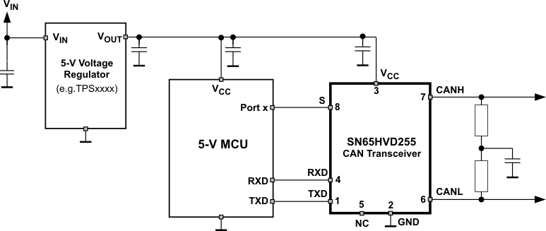 Figure 17. Typical 5-V Application
10.2.1.1 Design Requirements
10.2.1.1.1 CAN Termination
The ISO11898 standard specifies the interconnect to be a twisted-pair cable (shielded or unshielded) with 120-Ω characteristic impedance (ZO). Resistors equal to the characteristic impedance of the line must be used to terminate both ends of the cable to prevent signal reflections. Unterminated drop lines (stubs) connecting nodes to the bus must be kept as short as possible to minimize signal reflections. The termination may be on the cable or in a node, but if nodes may be removed from the bus, the termination must be carefully placed so that it is not removed from the bus.
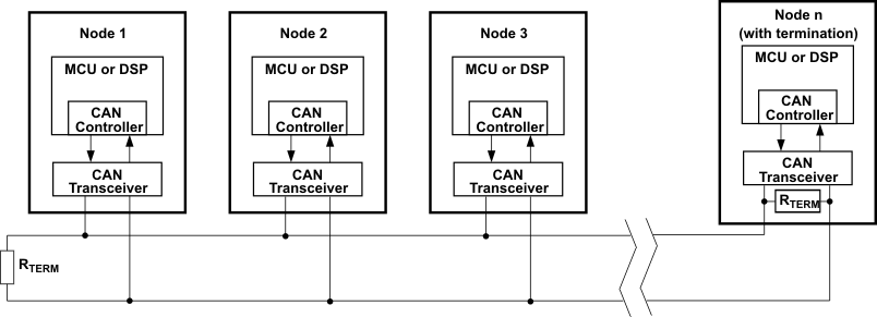 Figure 18. Typical CAN Bus
Termination may be a single 120-Ω resistor at the end of the bus either on the cable or in a terminating node. If filtering and stabilization of the common mode voltage of the bus is desired, then split termination may be used (see Figure 19). Split termination improves the electromagnetic emissions behavior of the network by eliminating fluctuations in the bus common-mode voltages at the start and end of message transmissions.
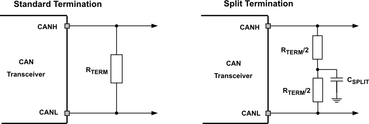 Figure 19. CAN Bus Termination Concepts
10.2.1.2 Detailed Design Procedure
10.2.1.2.1 Example: Functional Safety Using the SN65HVD257 in a Redundant Physical Layer CAN Network Topology
CAN is a standard linear bus topology using 120-Ω twisted-pair cabling. The SN65HVD257 CAN device includes several features to use the CAN physical layer in nonstandard topologies with only one CAN link layer controller (μP) interface. This allows much greater flexibility in the physical topology of the bus while reducing the digital controller and software costs. The combination of RXD DTO and the FAULT output allows great flexibility, control, and monitoring of these applications.
A simple example of this flexibility is to use two SN65HVD257 devices in parallel with an AND gate to achieve redundancy (parallel) of the physical layer (cabling and PHYs) in a CAN network.
For the CAN bit-wise arbitration to work, the RXD outputs of the transceivers must connect through AND gate logic so that a dominant bit (low) from any of the branches is received by the link layer logic (μP) and appears to the link layer and above as a single physical network. The RXD DTO feature prevents a bus stuck dominant fault in a single branch from taking down the entire network by forcing the RXD pin for the transceivers on the branch with the fault back to the recessive after the tRXD_DTO time. The remaining branch of the network continues to function. The FAULT pin of the transceivers on the branch with the fault indicates this through the FAULT output to their host processors, which diagnose the failure condition. The S pin (silent mode pin) may be used to put a branch in silent mode to check each branch for other faults. Therefore, it is possible to implement a robust and redundant CAN network topology in a very simple and low-cost manner.
These concepts can be expanded into more complicated and flexible CAN network topologies to solve various system-level challenges with a networked infrastructure.

10.2.1.3 Application Curves
Figure 21 shows the typical loop delay through the transceiver based on the differential resistive load between CANH and CANL.
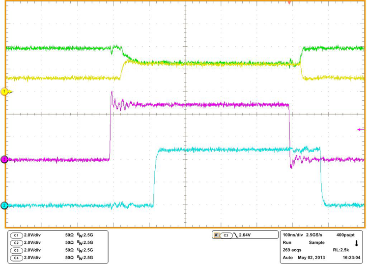 Figure 21. Typical TXD to RXD Loop Delay
10.2.2 Typical 3.3-V Microcontroller Application
The SN65HVD256 device has a second supply voltage pin used for level shifting the input and output pins. This can be used for applications where there is a 3.3-V micrcontroller and a 5-V CAN transceiver.
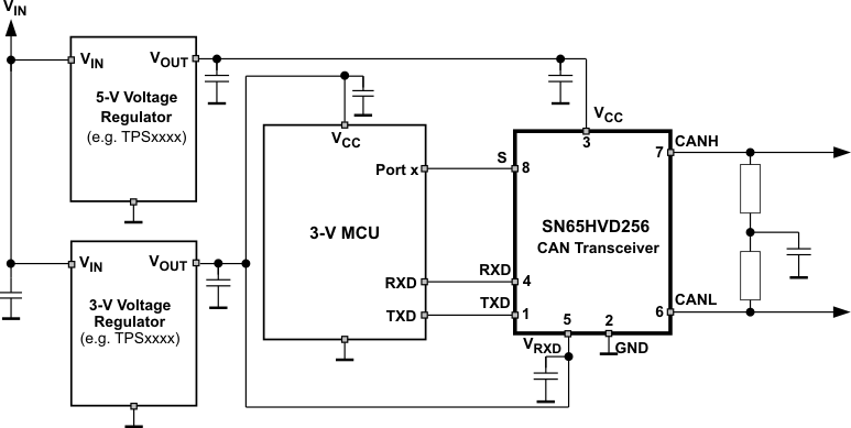 Figure 22. Typical 3.3-V Application