SLLS994B February 2010 – July 2015 SN65HVDA1050A-Q1
PRODUCTION DATA.
- 1 Features
- 2 Applications
- 3 Description
- 4 Revision History
- 5 Pin Configuration and Functions
- 6 Specifications
- 7 Parameter Measurement Information
- 8 Detailed Description
- 9 Application and Implementation
- 10Power Supply Recommendations
- 11Layout
- 12Device and Documentation Support
- 13Mechanical, Packaging, and Orderable Information
Package Options
Mechanical Data (Package|Pins)
- D|8
Thermal pad, mechanical data (Package|Pins)
Orderable Information
8 Detailed Description
8.1 Overview
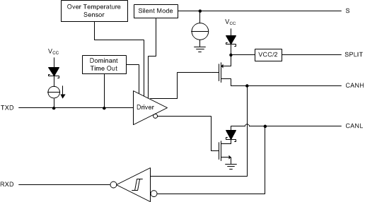
The SN65HVDA1050A-Q1 CAN transceiver is compatible with the ISO 11898-2 high-speed controller area network (CAN) physical layer standard. The device is designed to interface between the differential bus lines in controller area network and the CAN protocol controller at data rates up to 1 Mbps.
8.2 Functional Block Diagram

8.3 Feature Description
8.3.1 Operating Modes
The device has two main operating modes: normal mode and silent mode. Operating mode selection is made through the S input pin.
Table 2. Operating Modes
| S PIN | MODE | DRIVER | RECEIVER | RXD PIN |
|---|---|---|---|---|
| LOW | Normal | Enabled (On) | Enabled (On) | Mirrors CAN bus |
| HIGH | Silent | Disabled (Off) | Enabled (On) | Mirrors CAN bus |
8.3.1.1 Normal Mode
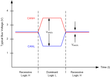
This is the normal operating mode of the device. Normal mode is selected by setting S low. The CAN driver and receiver are fully operational and CAN communication is bidirectional. The driver is translating a digital input on TXD to a differential output on CANH and CANL. The receiver is translating the differential signal from CANH and CANL to a digital output on RXD. In recessive state, the bus pins are biased to 0.5 × VCC. In dominant state, the bus pins (CANH and CANL) are driven differentially apart. Logic high is equivalent to recessive on the bus and logic low is equivalent to a dominant (differential) signal on the bus.
 Figure 14. Bus Logic-State Voltage Definitions
The SPLIT (VREF) pin is biased to 0.5 × VCC for bus common mode bus voltage bias stabilization in split termination network applications (see Application and Implementation).
8.3.1.2 Silent Mode
Silent mode disables the driver (transmitter) of the device; however, the receiver still operates and translates the differential signal from CANH and CANL to the digital output on RXD. It is selected by setting S high. The bus pins (CANH and CANL) are biased to 0.5 × VCC. The SPLIT (VREF) pin is biased to 0.5 × VCC.
8.3.2 Protection Features
8.3.2.1 TXD Dominant State Timeout
During normal mode operation (the only mode where the CAN driver is active), the TXD dominant time-out circuit prevents the transceiver from blocking network communication in the event of a hardware or software failure where TXD is held dominant longer than the time-out period, tDST. The dominant time-out circuit is triggered by a falling edge on TXD. If no rising edge occurs before the time-out constant of the circuit expires (tDST), the CAN bus driver is disabled, thus freeing the bus for communication between other network nodes. The CAN driver is reactivated when a recessive signal occurs on the TXD pin, thus clearing the dominant-state time-out. The CAN bus pins are biased to recessive level during a TXD dominant-state time-out, and SPLIT (VREF) remains on.
NOTE
The maximum dominant TXD time allowed by the TXD dominant state time-out limits the minimum possible data rate of the device. The CAN protocol allows a maximum of eleven successive dominant bits (on TXD) for the worst case, where five successive dominant bits are followed immediately by an error frame. This, along with the t(dom) minimum, limits the minimum bit rate. The minimum bit rate may be calculated by:
Minimum Bit Rate = 11 / t(dom)
8.3.2.2 Thermal Shutdown
If the junction temperature of the device exceeds the thermal-shutdown threshold, the device turns off the CAN driver circuits. The SPLIT (VREF) pin remains biased. This condition is cleared when the temperature drops below the thermal-shutdown temperature of the device.
8.3.2.3 Undervoltage Lockout and Unpowered Device
The device has undervoltage detection and lockout on the VCC supply. If an undervoltage condition is detected on VCC, the device protects the bus.
The TXD pin is pulled up to VCC to force a recessive input level if the pin floats. The S pin is pulled up to GND to force the device into normal mode if the pin floats.
The bus pins [CANH, CANL, and SPLIT (VREF)] all have low leakage currents when the device is unpowered.
8.4 Device Functional Modes
Table 3. Driver Function Table(1)
| INPUTS | OUTPUTS | BUS STATE | ||
|---|---|---|---|---|
| TXD | S | CANH | CANL | |
| L | L or Open | H | L | Dominant |
| H | X | Z | Z | Recessive |
| Open | X | Z | Z | Recessive |
| X | H | Z | Z | Recessive |
Table 4. Receiver Function Table(1)
| DIFFERENTIAL INPUTS VID = V(CANH) – V(CANL) |
OUTPUT RXD |
BUS STATE |
|---|---|---|
| VID ≥ 0.9 V | L | Dominant |
| 0.5 V < VID < 0.9 V | ? | ? |
| VID ≤ 0.5 V | H | Recessive |
| Open | H | Recessive |