SLLS530C April   2002  – February 2019 SN65LVDT14 , SN65LVDT41

PRODUCTION DATA.  

  1. Features
  2. Applications
  3. Description
    1.     Device Images
      1.      SN65LVDT41 Functional Diagram
      2.      SN65LVDT14 Functional Diagram
  4. Revision History
  5. Pin Configuration and Functions
    1.     SN65LVDT41 Pin Functions
    2.     SN65LVDT14 Pin Functions
  6. Specifications
    1. 6.1  Absolute Maximum Ratings
    2. 6.2  ESD Ratings
    3. 6.3  Recommended Operating Conditions
    4. 6.4  Thermal Information
    5. 6.5  Receiver Electrical Characteristics
    6. 6.6  Driver Electrical Characteristics
    7. 6.7  Device Electrical Characteristics
    8. 6.8  Receiver Switching Characteristics
    9. 6.9  Driver Switching Characteristics
    10. 6.10 Typical Characteristics
      1. 6.10.1 Receiver
      2. 6.10.2 Driver
  7. Parameter Measurement Information
  8. Detailed Description
    1. 8.1 Overview
    2. 8.2 Functional Block Diagram
    3. 8.3 Feature Description
      1. 8.3.1 SN65LVDTxx Driver and Receiver Functionality
      2. 8.3.2 Integrated Termination
      3. 8.3.3 SN65LVDTxx Equivalent Circuits
    4. 8.4 Device Functional Modes
  9. Application and Implementation
    1. 9.1 Application Information
      1. 9.1.1 Extending a Serial Peripheral Interface Using LVDS Signaling Over Differential Transmission Cables
    2. 9.2 Typical Application
      1. 9.2.1 Design Requirements
      2. 9.2.2 Detailed Design Procedure
        1. 9.2.2.1 SPI Propagation Delay Limitations
        2. 9.2.2.2 Interconnecting Media
        3. 9.2.2.3 Input Fail-Safe Biasing
        4. 9.2.2.4 Power Decoupling Recommendations
        5. 9.2.2.5 PCB Transmission Lines
        6. 9.2.2.6 Probing LVDS Transmission Lines on PCB
      3. 9.2.3 Application Curve
  10. 10Power Supply Recommendations
  11. 11Layout
    1. 11.1 Layout Guidelines
      1. 11.1.1 Microstrip vs. Stripline Topologies
      2. 11.1.2 Dielectric Type and Board Construction
      3. 11.1.3 Recommended Stack Layout
      4. 11.1.4 Separation Between Traces
      5. 11.1.5 Crosstalk and Ground Bounce Minimization
      6. 11.1.6 Decoupling
    2. 11.2 Layout Examples
  12. 12Device and Documentation Support
    1. 12.1 Related Documentation
    2. 12.2 Receiving Notification of Documentation Updates
    3. 12.3 Related Links
    4. 12.4 Community Resources
    5. 12.5 Trademarks
    6. 12.6 Electrostatic Discharge Caution
    7. 12.7 Glossary
  13. 13Mechanical, Packaging, and Orderable Information

Package Options

Refer to the PDF data sheet for device specific package drawings

Mechanical Data (Package|Pins)
  • PW|20
Thermal pad, mechanical data (Package|Pins)
Orderable Information

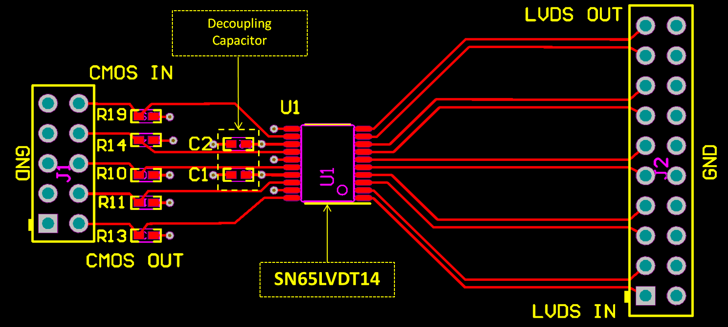
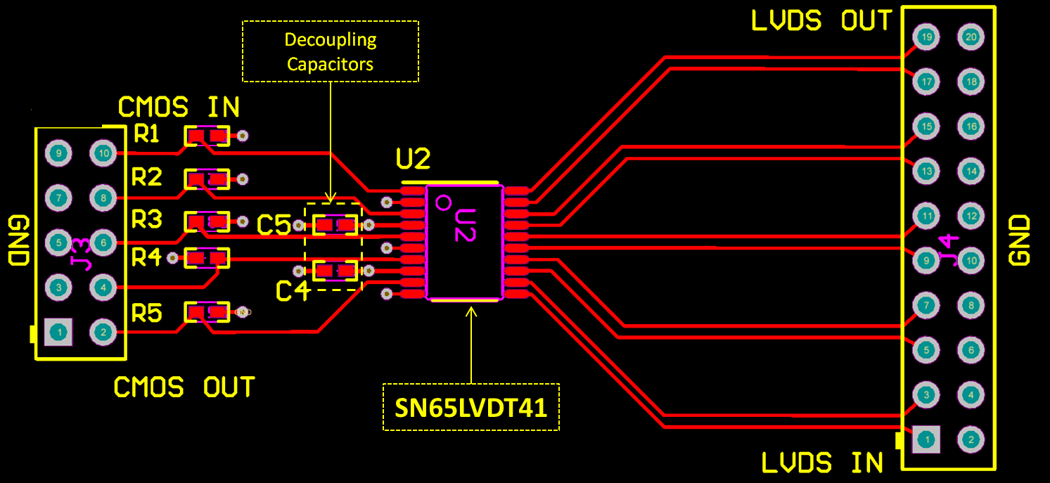
Layout Examples

SN65LVDT14 SN65LVDT41 LayoutExample_LVDT14.pngFigure 32. Example SN65LVDT14 Layout
SN65LVDT14 SN65LVDT41 LayoutExample_LVDT41.pngFigure 33. Example SN65LVDT41