SLLSFG7B September 2020 – November 2022 SN65MLVD203B
PRODUCTION DATA
- 1 Features
- 2 Applications
- 3 Description
- 4 Revision History
- 5 Pin Configuration and Functions
-
6 Specifications
- 6.1 Absolute Maximum Ratings
- 6.2 ESD Ratings
- 6.3 Recommended Operating Conditions
- 6.4 Thermal Information
- 6.5 Electrical Characteristics
- 6.6 Electrical Characteristics – Driver
- 6.7 Electrical Characteristics – Receiver
- 6.8 Switching Characteristics – Driver
- 6.9 Switching Characteristics – Receiver
- 6.10 Typical Characteristics
- 7 Parameter Measurement Information
- 8 Detailed Description
-
9 Application and Implementation
- 9.1 Application Information
- 9.2
Typical Application
- 9.2.1 Multipoint Communications
- 9.2.2 Design Requirements
- 9.2.3
Detailed Design Procedure
- 9.2.3.1 Supply Voltage
- 9.2.3.2 Supply Bypass Capacitance
- 9.2.3.3 Driver Input Voltage
- 9.2.3.4 Driver Output Voltage
- 9.2.3.5 Termination Resistors
- 9.2.3.6 Receiver Input Signal
- 9.2.3.7 Receiver Input Threshold (Failsafe)
- 9.2.3.8 Receiver Output Signal
- 9.2.3.9 Interconnecting Media
- 9.2.3.10 PCB Transmission Lines
- 9.2.4 Application Curves
- 9.3 Power Supply Recommendations
- 9.4 Layout
- 10Device and Documentation Support
- 11Mechanical, Packaging, and Orderable Information
Package Options
Mechanical Data (Package|Pins)
- RUM|16
Thermal pad, mechanical data (Package|Pins)
- RUM|16
Orderable Information
9.2.3.2 Supply Bypass Capacitance
Bypass capacitors play a key role in power distribution circuitry. At low frequencies, power supply offers very low-impedance paths between its terminals. However, as higher frequency currents propagate through power traces, the source is often incapable of maintaining a low-impedance path to ground. Bypass capacitors are used to address this shortcoming. Usually, large bypass capacitors (10 μF to 1000 μF) at the board level do a good job up into the kHz range. Due to their size and length of their leads, large capacitors tend to have large inductance values at the switching frequencies. To solve this problem, smaller capacitors (in the nF to μF range) must be installed locally next to the integrated circuit.
Multilayer ceramic chip or surface-mount capacitors (size 0603 or 0805) minimize lead inductances of bypass capacitors in high-speed environments, because their lead inductance is about 1 nH. For comparison purposes, a typical capacitor with leads has a lead inductance around 5 nH.
The value of the bypass capacitors used locally with M-LVDS chips can be determined by Equation 1 and Equation 2, according to High Speed Digital Design – A Handbook of Black Magic by Howard Johnson and Martin Graham (1993). A conservative rise time of 4 ns and a worst-case change in supply current of 100 mA covers the whole range of M-LVDS devices offered by Texas Instruments. In this example, the maximum power supply noise tolerated is 100 mV; however, this figure varies depending on the noise budget available for the design.
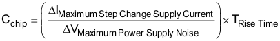
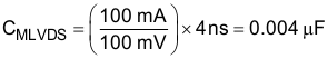
Figure 9-2 shows a configuration that lowers lead inductance and covers intermediate frequencies between the board-level capacitor (>10 µF) and the value of capacitance found above (0.004 µF). Place the smallest value of capacitance as close as possible to the chip.
 Figure 9-2 Recommended M-LVDS Bypass Capacitor Layout