SLLSFG7B September 2020 – November 2022 SN65MLVD203B
PRODUCTION DATA
- 1 Features
- 2 Applications
- 3 Description
- 4 Revision History
- 5 Pin Configuration and Functions
-
6 Specifications
- 6.1 Absolute Maximum Ratings
- 6.2 ESD Ratings
- 6.3 Recommended Operating Conditions
- 6.4 Thermal Information
- 6.5 Electrical Characteristics
- 6.6 Electrical Characteristics – Driver
- 6.7 Electrical Characteristics – Receiver
- 6.8 Switching Characteristics – Driver
- 6.9 Switching Characteristics – Receiver
- 6.10 Typical Characteristics
- 7 Parameter Measurement Information
- 8 Detailed Description
-
9 Application and Implementation
- 9.1 Application Information
- 9.2
Typical Application
- 9.2.1 Multipoint Communications
- 9.2.2 Design Requirements
- 9.2.3
Detailed Design Procedure
- 9.2.3.1 Supply Voltage
- 9.2.3.2 Supply Bypass Capacitance
- 9.2.3.3 Driver Input Voltage
- 9.2.3.4 Driver Output Voltage
- 9.2.3.5 Termination Resistors
- 9.2.3.6 Receiver Input Signal
- 9.2.3.7 Receiver Input Threshold (Failsafe)
- 9.2.3.8 Receiver Output Signal
- 9.2.3.9 Interconnecting Media
- 9.2.3.10 PCB Transmission Lines
- 9.2.4 Application Curves
- 9.3 Power Supply Recommendations
- 9.4 Layout
- 10Device and Documentation Support
- 11Mechanical, Packaging, and Orderable Information
Package Options
Mechanical Data (Package|Pins)
- RUM|16
Thermal pad, mechanical data (Package|Pins)
- RUM|16
Orderable Information
9.4.2 Layout Example
At least two or three times the width of an individual trace should separate single-ended traces and differential pairs to minimize the potential for crosstalk. Single-ended traces that run in parallel for less than the wavelength of the rise or fall times usually have negligible crosstalk. Increase the spacing between signal paths for long parallel runs to reduce crosstalk. Boards with limited real estate can benefit from the staggered trace layout, as shown in Figure 9-13.
 Figure 9-13 Staggered
Trace Layout
Figure 9-13 Staggered
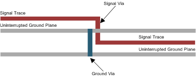
Trace LayoutThis configuration lays out alternating signal traces on different layers; thus, the horizontal separation between traces can be less than 2 or 3 times the width of individual traces. To ensure continuity in the ground signal path, TI recommends having an adjacent ground via for every signal via, as shown in Figure 9-14. Note that vias create additional capacitance. For example, a typical via has a lumped capacitance effect of 1/2 pF to 1 pF in FR4.
 Figure 9-14 Ground
Via Location (Side View)
Figure 9-14 Ground
Via Location (Side View)Short and low-impedance connection of the device ground pins to the PCB ground plane reduces ground bounce. Holes and cutouts in the ground planes can adversely affect current return paths if they create discontinuities that increase returning current loop areas.
To minimize EMI problems, TI recommends avoiding discontinuities below a trace (for example, holes, slits, and so on) and keeping traces as short as possible. Zoning the board wisely by placing all similar functions in the same area, as opposed to mixing them together, helps reduce susceptibility issues.