SCAS294O JANUARY 1993 – June 2015 SN54LVC257A , SN74LVC257A
PRODUCTION DATA.
- 1 Features
- 2 Applications
- 3 Description
- 4 Revision History
- 5 Device Options
- 6 Pin Configuration and Functions
-
7 Specifications
- 7.1 Absolute Maximum Ratings
- 7.2 ESD Ratings
- 7.3 Recommended Operating Conditions
- 7.4 Thermal Information: 16-Pin Packages
- 7.5 Thermal Information: 20-Pin Package
- 7.6 Electrical Characteristics
- 7.7 SN54LVC257A Switching Characteristics
- 7.8 SN74LVC257A Switching Characteristics
- 7.9 Operating Characteristics
- 7.10 Typical Characteristics
- 8 Parameter Measurement Information
- 9 Detailed Description
- 10Application and Implementation
- 11Power Supply Recommendations
- 12Layout
- 13Device and Documentation Support
- 14Mechanical, Packaging, and Orderable Information
Package Options
Mechanical Data (Package|Pins)
Thermal pad, mechanical data (Package|Pins)
- RGY|16
Orderable Information
9 Detailed Description
9.1 Overview
These quadruple 2-line to 1-line data selectors and multiplexers are designed for 1.65-V to 3.6-V VCC operation.
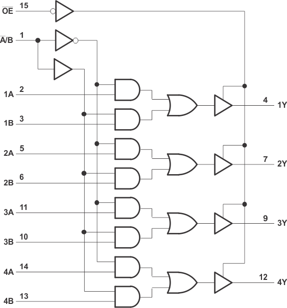
The SNx4LVC257A devices are designed to multiplex signals from 4-bit data sources to 4-output data lines in bus-organized systems. The 3-state outputs do not load the data lines when the output-enable (OE) input is at a high logic level.
9.2 Functional Block Diagram

9.3 Feature Description
Inputs can be driven from either 3.3-V or 5-V devices. This feature allows the use of these devices as translators in a mixed 3.3-V and 5-V system environment. Device features a maximum tpd of 4.6 ns allowing the device to be used in high-speed applications as well.
To ensure the high-impedance state during power up or power down, OE must be tied to VCC through a pullup resistor; the minimum value of the resistor is determined by the current-sinking capability of the driver.
9.4 Device Functional Modes
Table 1 lists the functional modes for the SN54LVC257A and SN74LVC257A devices.
Table 1. Function Table
| INPUTS | OUTPUT Y |
|||
|---|---|---|---|---|
| OE | A/B | A | B | |
| H | X | X | X | Z |
| L | L | L | X | L |
| L | L | H | X | H |
| L | H | X | L | L |
| L | H | X | H | H |