SCAS298N January 1993 – June 2014 SN54LVC541A , SN74LVC541A
PRODUCTION DATA.
- 1 Features
- 2 Applications
- 3 Description
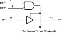
- 4 Simplified Schematic
- 5 Revision History
- 6 Pin Configuration and Functions
-
7 Specifications
- 7.1 Absolute Maximum Ratings
- 7.2 Handling Ratings
- 7.3 Recommended Operating Conditions
- 7.4 Thermal Information
- 7.5 Electrical Characteristics—DC Limit Changes
- 7.6 Switching Characteristics—AC Limit Changes
- 7.7 Switching Characteristics, SN74LVC541A -40°C to 85°C
- 7.8 Switching Characteristics, SN74LVC541A -40°C to 125°C
- 7.9 Operating Characteristics
- 7.10 Typical Characteristics
- 8 Parameter Measurement Information
- 9 Detailed Description
- 10Application and Implementation
- 11Power Supply Recommendations
- 12Layout
- 13Device and Documentation Support
- 14Mechanical, Packaging, and Orderable Information
Package Options
Refer to the PDF data sheet for device specific package drawings
Mechanical Data (Package|Pins)
- DGV|20
- DB|20
- NS|20
- DW|20
- PW|20
- RGY|20
Thermal pad, mechanical data (Package|Pins)
- RGY|20
Orderable Information
1 Features
- Operate From 1.65 V to 3.6 V
- Inputs Accept Voltages to 5.5 V
- Max tpd of 5.1 ns at 3.3 V
- Typical VOLP (Output Ground Bounce)
<0.8 V at VCC = 3.3 V, TA = 25°C - Typical VOHV (Output VOH Undershoot)
>2 V at VCC = 3.3 V, TA = 25°C - Support Mixed-Mode Signal Operation on
All Ports (5-V Input/Output Voltage With
3.3-V VCC) - Ioff Supports Live Insertion, Partial-Power-Down Mode, and Back-Drive Protection
- Latch-Up Performance Exceeds 250 mA
Per JESD 17 - ESD Protection Exceeds JESD 22
- 2000-V Human-Body Model (A114-A)
- 200-V Machine Model (A115-A)
- 1000-V Charged-Device Model (C101)
-
On Products Compliant to MIL-PRF-38535,
All Parameters Are Tested Unless Otherwise Noted. On All Other Products, Production Processing Does Not Necessarily Include Testing of All Parameters.
2 Applications
3 Description
The SN54LVC541A octal buffer/driver is designed for 2.7-V to 3.6-V VCC operation, and the SN74LVC541A octal buffer/driver is designed for 1.65-V to 3.6-V VCC operation.
Device Information(1)
| PART NUMBER | PACKAGE | BODY SIZE (NOM) |
|---|---|---|
| SN74LVC541A | SSOP (20) | 7.20 mm × 5.30 mm |
| TVSOP (20) | 5.00 mm × 4.40 mm | |
| VQFN (20) | 4.50 mm × 3.50 mm | |
| SOIC (20) | 12.80 mm × 7.50 mm | |
| TSSOP (20) | 6.50 mm × 4.40 mm |
- For all available packages, see the orderable addendum at the end of the data sheet.
4 Simplified Schematic