SCAS298N January 1993 – June 2014 SN54LVC541A , SN74LVC541A
PRODUCTION DATA.
- 1 Features
- 2 Applications
- 3 Description
- 4 Simplified Schematic
- 5 Revision History
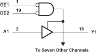
- 6 Pin Configuration and Functions
-
7 Specifications
- 7.1 Absolute Maximum Ratings
- 7.2 Handling Ratings
- 7.3 Recommended Operating Conditions
- 7.4 Thermal Information
- 7.5 Electrical Characteristics—DC Limit Changes
- 7.6 Switching Characteristics—AC Limit Changes
- 7.7 Switching Characteristics, SN74LVC541A -40°C to 85°C
- 7.8 Switching Characteristics, SN74LVC541A -40°C to 125°C
- 7.9 Operating Characteristics
- 7.10 Typical Characteristics
- 8 Parameter Measurement Information
- 9 Detailed Description
- 10Application and Implementation
- 11Power Supply Recommendations
- 12Layout
- 13Device and Documentation Support
- 14Mechanical, Packaging, and Orderable Information
Package Options
Refer to the PDF data sheet for device specific package drawings
Mechanical Data (Package|Pins)
- DGV|20
- DB|20
- NS|20
- DW|20
- PW|20
- RGY|20
Thermal pad, mechanical data (Package|Pins)
- RGY|20
Orderable Information
9 Detailed Description
9.1 Overview
The 'LVC541A devices are ideal for driving bus lines or buffering memory address registers.
These devices feature inputs and outputs on opposite sides of the package to facilitate printed circuit board layout. The 3-state control gate is a 2-input AND gate with active-low inputs so that, if either output enable (OE1 or OE2) input is high, all eight outputs are in the high-impedance state. Inputs can be driven from either 3.3-V or 5-V devices. This feature allows the use of these devices as translators in a mixed 3.3-V/5-V system environment. These devices are fully specified for partial-power-down applications using Ioff. The Ioff circuitry disables the outputs, preventing damaging current backflow through the devices when they are powered down. To ensure the high-impedance state during power up or power down, OE should be tied to VCC through a pullup resistor; the minimum value of the resistor is determined by the current-sinking capability of the driver.
9.2 Functional Block Diagram
9.3 Feature Description
- Wide operating voltage range
- Operates from 1.65 V to 3.6 V
- Allows down voltage translation
- Inputs accept voltages to 5.5 V
- Ioff feature
- Allows voltages on the inputs and outputs when VCC is 0 V
9.4 Device Functional Modes
Table 1. Function Table
| INPUTS | OUTPUT Y |
||
|---|---|---|---|
| OE1 | OE2 | A | |
| L | L | L | L |
| L | L | H | H |
| H | X | X | Z |
| X | H | X | Z |