SLLS009E October 1985 – March 2024 SN75ALS194
PRODUCTION DATA
- 1
- 1 Features
- 2 Applications
- 3 Description
- 4 Pin Configuration and Functions
- 5 Specifications
- 6 Parameter Measurement Information
- 7 Detailed Description
- 8 Device and Documentation Support
- 9 Revision History
- 10Mechanical, Packaging, and Orderable Information
Package Options
Refer to the PDF data sheet for device specific package drawings
Mechanical Data (Package|Pins)
- NS|16
- N|16
- D|16
Thermal pad, mechanical data (Package|Pins)
Orderable Information
5.6 Switching Characteristics
VCC = 5V, TA = 25°C
| PARAMETER | TEST CONDITIONS | SN75ALS194 | UNIT | |||
|---|---|---|---|---|---|---|
| MIN | TYP | MAX | ||||
| tPLH | Propagation delay time, low- to high-level output | C 15 F L = 15pF, See Figure 6-1 | 6 | 13 | ns | |
| tPHL | Propagation delay time, high- to low-level output | 9 | 14 | ns | ||
| Output-to-output skew | 3.5 | 6 | ns | |||
| tt(OD) | Differential output transition time | CL = 15pF, See Figure 6-2 | 8 | 14 | ns | |
| tPZH | Output enable time to high level | CL = 15pF, See Figure 6-3 | 9 | 12 | ns | |
| tPZL | Output enable time to low level | 12 | 20 | ns | ||
| tPHZ | Output disable time from high level | 9 | 14 | ns | ||
| tPLZ | Output disable time from low level | 12 | 15 | ns | ||
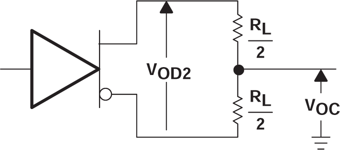
Table 5-1 Symbol Equivalents
| DATA SHEET PARAMETER | EIA/TIA-422-B |
|---|---|
| VO | Voa, Vob |
| | VOD1 | | Vo |
| | VOD2 | | Vt (RL = 100 Ω) |
| ∆ | VOD | | | |Vt| – |V t| | |
| VOC | | Vos | |
| ∆ | VOC | | | Vos – V os | |
| IOS | |Isa|, |Isb| |
| IO | |Ixa| , |Ixb| |
 Figure 5-1 Driver VOD And VOC