SLLSEA9B February 2012 – August 2015 SN75DP126
PRODUCTION DATA.
- 1 Features
- 2 Applications
- 3 Description
- 4 Revision History
- 5 Description (continued)
- 6 Pin Configuration and Functions
-
7 Specifications
- 7.1 Absolute Maximum Ratings
- 7.2 ESD Ratings
- 7.3 Recommended Operating Conditions
- 7.4 Thermal Information
- 7.5 Power Supply Electrical Characteristics
- 7.6 Main Link Input Electrical Characteristics
- 7.7 DisplayPort Main Link Output Electrical Characteristics
- 7.8 HDMI/DVI Main Link Output Electrical Characteristics
- 7.9 HPD/CAD/EN Electrical Characteristics
- 7.10 AUX/DDC/I2C Electrical Characteristics
- 7.11 DisplayPort Main Link Output Switching Characteristics
- 7.12 HDMI/DVI Main Link Switching Characteristics
- 7.13 HPD/CAD Switching Characteristics
- 7.14 AUX/DDC/I2C Switching Characteristics
- 7.15 Typical Characteristics
-
8 Detailed Description
- 8.1 Overview
- 8.2 Functional Block Diagram
- 8.3
Feature Description
- 8.3.1 Implementing the EN Signal
- 8.3.2 Hot Plug Detect (HPD) and Cable Adapter Detect (CAD) Description
- 8.3.3 OVS Function Description
- 8.3.4 AUX and DDC Configuration Details
- 8.3.5 Source-Side Main Link EQ Configuration Details
- 8.3.6 DP-HDMI Adaptor ID Buffer
- 8.3.7 GPU with a Unified AUX/DDC Configuration
- 8.3.8 GPU with Separate DDC and AUX Channels
- 8.4 Device Functional Modes
- 8.5 Register Maps
- 9 Application and Implementation
- 10Power Supply Recommendations
- 11Layout
- 12Device and Documentation Support
- 13Mechanical, Packaging, and Orderable Information
Package Options
Mechanical Data (Package|Pins)
- RHU|56
Thermal pad, mechanical data (Package|Pins)
Orderable Information
1 Features
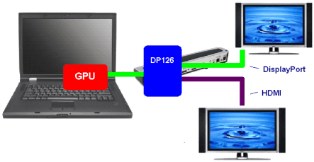
- One Dual-Mode DisplayPort™ (DP++) Input; Switchable to One DP++ Output or One TMDS Output Compatible with HDMI 1.4b and DVI
- Supports DP v1.1a and DP v1.2 Signaling Including HBR2 Data Rates to 5.4 Gbps
- Supports HDMI 1.4b with TMDS Clock Frequencies up to 340 MHz with 10 m Cable
- Glue-less interface to AMD, Intel, and NVIDIA Graphics Processors
- Auto-Configuration Through Link Training for DisplayPort Connection
- Integrated DDC-Accessible DP-HDMI Adaptor ID for HDMI/DVI Sink Recognition
- Output Signal Conditioning with Tunable Voltage Swing and Pre-Emphasis Gain for both DisplayPort and TMDS Outputs
- Highly-Configurable Input-Variable Equalizer
- Two Device Options Including a Dual Power-Supply Configuration for Lowest Power
- 2-kV ESD HBM Protection
- Temperature Range: 0°C to 85°C
- 56-Pin 5-mm x 11-mm QFN Package
2 Applications
- Notebook PC
- Desktop PC
- PC Docking Station
- PC Standalone Video Card
3 Description
The SN75DP126 switches one Dual-Mode DisplayPort (DP++) input to one Dual-Mode DisplayPort (DP++) sink output or one HDMI/DVI sink output. The HDMI/DVI output has a built-in level translator compliant with DVI 1.0 and HDMI 1.4b standard TMDS signaling, and is specified up to a maximum data rate of 3.4 Gbps, supporting resolutions greater than 1920 X 1440 and HDTV deep color at 1080p. An integrated DP-HDMI Adaptor ID buffer can be accessed when the HDMI/DVI sink is selected to indicate support for HDMI signaling.
The device compensates for PCB-related frequency loss and switching-related loss to provide the optimum electrical performance from source to sink. The DP++ Main Link signal inputs feature-configurable equalizers with selectable boost settings.
At the SN75DP126 DP++ Main Link output, four primary levels of differential output voltage (VOD) swing and four primary levels of pre-emphasis are available as well as a secondary level of boost adjustment, programmed through I2C, for fine-tuning the Main Link output. The device can monitor the AUX channel and automatically adjust output signaling levels and input equalizers based on DP Link Training commands.
Device Information(1)
| PART NUMBER | PACKAGE | BODY SIZE (NOM) |
|---|---|---|
| SN75DP126 | WQFN (56) | 11.00 mm × 5.00 mm |
- For all available packages, see the orderable addendum at the end of the datasheet.
Typical Application
