SLLSEA9B February 2012 – August 2015 SN75DP126
PRODUCTION DATA.
- 1 Features
- 2 Applications
- 3 Description
- 4 Revision History
- 5 Description (continued)
- 6 Pin Configuration and Functions
-
7 Specifications
- 7.1 Absolute Maximum Ratings
- 7.2 ESD Ratings
- 7.3 Recommended Operating Conditions
- 7.4 Thermal Information
- 7.5 Power Supply Electrical Characteristics
- 7.6 Main Link Input Electrical Characteristics
- 7.7 DisplayPort Main Link Output Electrical Characteristics
- 7.8 HDMI/DVI Main Link Output Electrical Characteristics
- 7.9 HPD/CAD/EN Electrical Characteristics
- 7.10 AUX/DDC/I2C Electrical Characteristics
- 7.11 DisplayPort Main Link Output Switching Characteristics
- 7.12 HDMI/DVI Main Link Switching Characteristics
- 7.13 HPD/CAD Switching Characteristics
- 7.14 AUX/DDC/I2C Switching Characteristics
- 7.15 Typical Characteristics
-
8 Detailed Description
- 8.1 Overview
- 8.2 Functional Block Diagram
- 8.3
Feature Description
- 8.3.1 Implementing the EN Signal
- 8.3.2 Hot Plug Detect (HPD) and Cable Adapter Detect (CAD) Description
- 8.3.3 OVS Function Description
- 8.3.4 AUX and DDC Configuration Details
- 8.3.5 Source-Side Main Link EQ Configuration Details
- 8.3.6 DP-HDMI Adaptor ID Buffer
- 8.3.7 GPU with a Unified AUX/DDC Configuration
- 8.3.8 GPU with Separate DDC and AUX Channels
- 8.4 Device Functional Modes
- 8.5 Register Maps
- 9 Application and Implementation
- 10Power Supply Recommendations
- 11Layout
- 12Device and Documentation Support
- 13Mechanical, Packaging, and Orderable Information
Package Options
Mechanical Data (Package|Pins)
- RHU|56
Thermal pad, mechanical data (Package|Pins)
Orderable Information
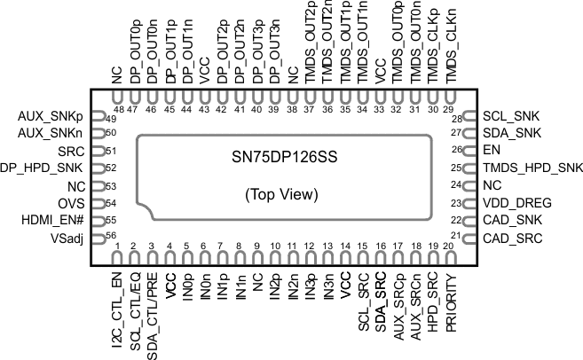
6 Pin Configuration and Functions
SN75DP126SS Single Supply RHU Package
56-Pin WQFN with Thermal Pad
Top View

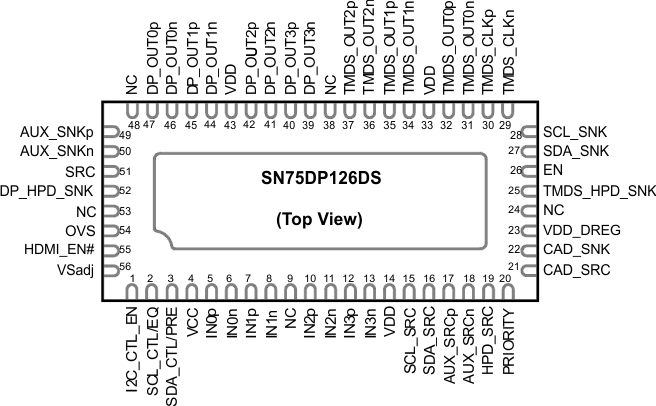
SN75DP126DS Dual Supply RHU Package
56-Pin WQFN with Thermal Pad
Top View

Pin Functions
| PIN | I/O | DESCRIPTION | |
|---|---|---|---|
| SIGNAL | NO. | ||
| DISPLAYPORT AND HDMI MAIN LINK TERMINALS | |||
| IN0p, IN0n | 5, 6 | 100Ω Differential Input |
DisplayPort Main Link Lane 0 Differential Input |
| IN1p, IN1n | 7, 8 | DisplayPort Main Link Lane 1 Differential Input | |
| IN2p, IN2n | 10, 11 | DisplayPort Main Link Lane 2 Differential Input | |
| IN3p, IN3n | 12, 13 | DisplayPort Main Link Lane 3 Differential Input | |
| DP_OUT0p, DP_OUT0n |
47, 46 | 100Ω Differential Output |
DisplayPort Main Link Lane 0 Differential Output |
| DP_OUT1p, DP_OUT1n |
45, 44 | DisplayPort Main Link Lane 1 Differential Output | |
| DP_OUT2p, DP_OUT2n |
42, 41 | DisplayPort Main Link Lane 2 Differential Output | |
| DP_OUT3p, DP_OUT3n |
40, 39 | DisplayPort Main Link Lane 3 Differential Output | |
| TMDS_CLKp, TMDS_CLKn |
30, 29 | 100Ω Differential Output (Failsafe) |
HDMI/DVI Clock TMDS Differential Output |
| TMDS_OUT0p, TMDS_OUT0n |
32, 31 | HDMI/DVI Data Lane 0 TMDS Differential Output | |
| TMDS_OUT1p, TMDS_OUT1n |
35, 34 | HDMI/DVI Data Lane 1 TMDS Differential Output | |
| TMDS_OUT2p, TMDS_OUT2n |
37, 36 | HDMI/DVI Data Lane 2 TMDS Differential Output | |
| AUX CHANNEL AND DDC DATA TERMINALS | |||
| AUX_SRCp, AUX_SRCn |
17, 18 | I/O (Failsafe) |
Source Side Bidirectional DisplayPort Auxiliary Data Channel. These signals are connected to the AUX_SNK channel when the DisplayPort sink is selected; AC coupling should be implemented. |
| AUX_SNKp, AUX_SNKn |
49, 50 | Sink Side Bidirectional DisplayPort Auxiliary Data Channel. | |
| SCL_SRC, SDA_SRC |
15, 16 | Source Side Bidirectional I2C Display Data Channel (DDC) for TMDS modes. These terminals include integrated 60 kΩ pull-up resistors. |
|
| SCL_SNK, SDA_SNK |
28, 27 | HDMI/DVI Sink Side Bidirectional I2C Display Data Channel (DDC). | |
| HOT PLUG DETECT AND CAD TERMINALS | |||
| HPD_SRC | 19 | Output | Hot Plug Detect Output to the Source. |
| This output shall be driven high when the source shall be connected to either the HDMI/DVI sink or the DisplayPort sink, and driven low when no sink is selected. This output will be asserted for a fixed period of time during active (PRIORITY based) transition from one sink to the other. | |||
| CAD_SRC | 21 | Source Side Cable Adapter Detect Output. When the DisplayPort sink is selected, this output represents the condition of the CAD_SNK input, active high as default; polarity may be programmed through the local I2C interface. When the HDMI/DVI sink is selected, this output is driven high. | |
| DP_HPD_SNK | 52 | Input (Failsafe) |
DisplayPort Hot Plug Detect Input from Sink. This device input is 5-V tolerant, and includes an integrated 130 kΩ pull-down resistor. Note: pull this input high during compliance testing or use I2C control interface to go into compliance test mode and control DP_HPD_SNK and HPD_SRC by software. |
| TMDS_HPD_SNK | 25 | HDMI/DVI Hot Plug Detect Input from Sink. This device input is 5-V tolerant, and includes an integrated 130 kΩ pull-down resistor. | |
| CAD_SNK | 22 | Input | DisplayPort Cable Adapter Detect Input. An external 1MΩ resistor to GND is recommended. This terminal is used to select DP mode (low input) or TMDS mode (high input) when the DisplayPort sink is selected . |
| CONTROL TERMINALS | |||
| VSadj | 56 | Input | HDMI/DVI Sink Differential Voltage Swing Control. An external resistor connecting this pin to GND determines the output voltage swing. A value of 4.7 kΩ is recommended to provide a typical swing of 1000 mV. VSadj resistor values of 4.7 kΩ ± 1 kΩ control the output voltage swing in a near-linear function of approximately 2 mV/100 Ω. Note: this input does not impact the output when a DisplayPort sink is selected and operating in TMDS mode (as supported by the DP++ source) |
| HDMI_EN# | 55 | HDMI/DVI Sink Type Control. When this input is low, the output is HDMI 1.4b compliant when the HDMI/DVI sink is selected. When this input is high, the output is DVI 1.0 compliant when the HDMI/DVI sink is selected. | |
| PRIORITY | 20 | Output Select Priority. Selects the priority for the output in the case both DP_HPD_SNK and TMDS_HPD_SNK are high indicating two sinks are connected. When low, the DisplayPort sink has priority selection. When high, the HDMI/DVI sink has priority. Note: An external RC circuit should be connected to the PRIORITY pin to insure that the SN76DP126 functions properly with some non-compliant monitors. See the SN75DP126 Reference Schematics for more information. |
|
| SRC | 51 | 3-Level Input |
TMDS Slew Rate Control. When the HDMI/DVI sink is selected, the slew rate is controlled by the HDMI_EN# input and by the SRC control input: |
| VIL = TMDS rise and fall times meet tT1 specifications | |||
| VIM (between VIL and VIH) = TMDS rise and fall times meet tT2 specifications (Recommended setting) | |||
| VIH = TMDS rise and fall times meet tT3 specifications | |||
| Note: this input does not impact the output when a DisplayPort sink is selected and operating in TMDS mode (as supported by the DP++ source) | |||
| OVS | 54 | 3-Level Input |
Source Side DDC Input/Output Buffer Control Input. When the HDMI/DVI sink is selected, the DDC VOL and VIL is controlled by the OVS control input: |
| VIL = Source DDC interface meets VOL(3) and VIL(3) specifications | |||
| VIM (between VIL and VIH) = Source DDC interface meets VOL(2) and VIL(2) specifications | |||
| VIH = Source DDC interface meets VOL(1) and VIL(1) specifications | |||
| I2C_CTL_EN | 1 | 3-Level Input |
Local I2C Interface Enable Control and Target Address Select. When low, the local I2C interface is disabled; when input is between VIL and VIH levels, the local I2C interface is enabled and is addressed at 0x58h (Write) and 0x59h (Read); when input is high, the local I2C interface is enabled and is addressed at 0x5Ah (Write) and 0x5Bh (Read). |
| SCL_CTL/EQ | 2 | 3-Level Input (Failsafe) |
Local I2C Interface Clock, or Equalizer Setting Control Input. When I2C_CTL_EN is input high or floating, this terminal is the local I2C interface clock used to configure SN75DP126. |
| When I2C_CTL_EN is low, this terminal can be used to configure the input EQ. | |||
| SDA_CTL/PRE | 3 | I/O 3-Level Input (Failsafe) |
Local I2C Interface Data, or TMDS Pre-emphasis Control Input. When I2C_CTL_EN is input high or floating, this terminal is the local I2C interface data signal. |
| When I2C_CTL_EN is low, this terminal configures the HDMI/DVI sink TMDS output pre-emphasis as: | |||
| VIL = 0 dB pre-emphasis applied to TMDS output | |||
| VIM = Not Recommended | |||
| VIH = 2 dB pre-emphasis applied to TMDS output | |||
| When 2 dB pre-emphasis is enabled, the steady state TMDS output swing is reduced from that selected by VSadj, and the transition time is reduced from that selected by SRC. | |||
| Note: this input does not impact the output when a DisplayPort sink is selected and operating in TMDS mode (as supported by the DP++ source), whereas no pre-emphasis is applied to the output signal in this condition. | |||
| EN | 26 | Low-Voltage Input (Failsafe) |
Device Enable / Reset (Power Down). This input incorporates internal pullup of 150 kΩ, and only 1.2-V tolerant (the high level shall be limited to 1.2 V). |
| When high, the device is enabled for normal operation. | |||
| When low, the device is in power down mode; all outputs excluding HPD_SRC and CAD_SRC are high-impedance, and inputs excluding DP_HPD_SNK, TMDS_HPD_SNK, and CAD_SNK are ignored; all local I2C and DPCD registers are reset to their default values when this input is low. | |||
| At power up, the EN input must not be de-asserted until the VCC supply has reached at least the minimum recommended supply voltage level. | |||
| SUPPLY AND GROUND TERMINALS | |||
| VCC | SN75DP126SS 4, 14, 33, 43 |
3.3-V Supply | |
| SN75DP126DS 4 |
|||
| VDD | SN75DP126DS 14, 33, 43 |
1.05-V Supply | |
| VDD_DREG | 23 | SN75DP126SS: Digital voltage regulator decoupling; install 1uF to GND. | |
| SN75DP126DS: Treat same as VDD; this pin will be most noisy of all VDD terminals and needs a de-coupling capacitor nearby. | |||
| GND | Exposed Thermal Pad | Ground. Reference GND connection shall be made to the exposed thermal pad. | |
| NC | 9, 53, 38, 48, 24 | No connect. These terminals may be left unconnected, or connect to GND. | |