SLLSEA9B February 2012 – August 2015 SN75DP126
PRODUCTION DATA.
- 1 Features
- 2 Applications
- 3 Description
- 4 Revision History
- 5 Description (continued)
- 6 Pin Configuration and Functions
-
7 Specifications
- 7.1 Absolute Maximum Ratings
- 7.2 ESD Ratings
- 7.3 Recommended Operating Conditions
- 7.4 Thermal Information
- 7.5 Power Supply Electrical Characteristics
- 7.6 Main Link Input Electrical Characteristics
- 7.7 DisplayPort Main Link Output Electrical Characteristics
- 7.8 HDMI/DVI Main Link Output Electrical Characteristics
- 7.9 HPD/CAD/EN Electrical Characteristics
- 7.10 AUX/DDC/I2C Electrical Characteristics
- 7.11 DisplayPort Main Link Output Switching Characteristics
- 7.12 HDMI/DVI Main Link Switching Characteristics
- 7.13 HPD/CAD Switching Characteristics
- 7.14 AUX/DDC/I2C Switching Characteristics
- 7.15 Typical Characteristics
-
8 Detailed Description
- 8.1 Overview
- 8.2 Functional Block Diagram
- 8.3
Feature Description
- 8.3.1 Implementing the EN Signal
- 8.3.2 Hot Plug Detect (HPD) and Cable Adapter Detect (CAD) Description
- 8.3.3 OVS Function Description
- 8.3.4 AUX and DDC Configuration Details
- 8.3.5 Source-Side Main Link EQ Configuration Details
- 8.3.6 DP-HDMI Adaptor ID Buffer
- 8.3.7 GPU with a Unified AUX/DDC Configuration
- 8.3.8 GPU with Separate DDC and AUX Channels
- 8.4 Device Functional Modes
- 8.5 Register Maps
- 9 Application and Implementation
- 10Power Supply Recommendations
- 11Layout
- 12Device and Documentation Support
- 13Mechanical, Packaging, and Orderable Information
Package Options
Mechanical Data (Package|Pins)
- RHU|56
Thermal pad, mechanical data (Package|Pins)
Orderable Information
9 Application and Implementation
NOTE
Information in the following applications sections is not part of the TI component specification, and TI does not warrant its accuracy or completeness. TI’s customers are responsible for determining suitability of components for their purposes. Customers should validate and test their design implementation to confirm system functionality.
9.1 Application Information
The SN75DP126 switches one Dual-Mode DisplayPort (DP++) input to one DP++ sink output or one HDMI/DVI sink output. The HDMI/DVI output has a built-in level translator compliant with DVI 1.0 and HDMI 1.4b and supports resolutions greater than 1920 x 1440 and HDTV deep color at 1080p.
9.2 Typical Application
The SN75DP126 can be used in a dongle implementation to switch from one DP++ Source to one DP++ Sink or one HDMI/DVI Sink.
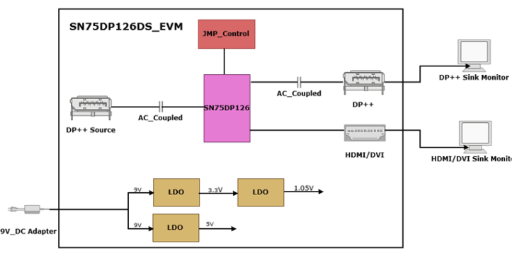 Figure 27. Typical Dongle Implementation
9.2.1 Design Requirements
The design requirements for this application are listed in Table 8.
Table 8. Design Requirements
| Design Parameter | Example Value |
|---|---|
| Source | DP++ |
| Sink | DP++ |
| Sink Priority | High (DP) |
| OVS | Low |
| PRE | Low |
| EQ | Low |
| SLEW | Low |
| VCC | 9 V |
9.2.2 Detailed Design Procedure
9.2.2.1 AC Coupling Capacitors
The DP link is an AC-coupled interface. AC coupling capacitors must be placed between the Source and the DP126.
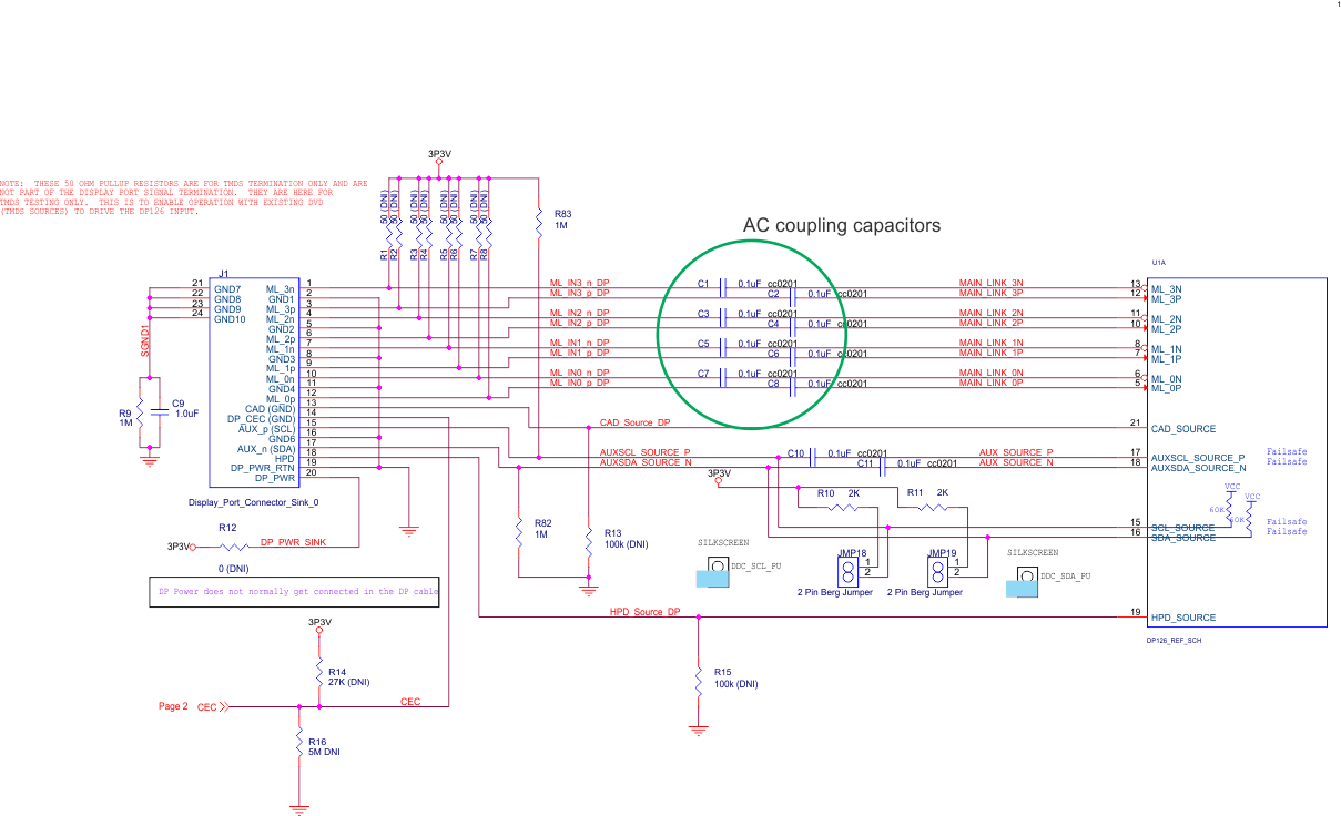 Figure 28. Source-to-DP126 AC Coupling Capacitors
AC coupling capacitors are required from the DP126 output to the DP Sink as well.
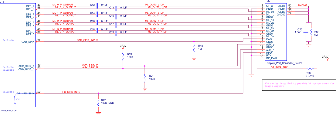 Figure 29. DP126 Output to the DP Sink AC Coupling Capacitors
9.2.2.2 Configuration Options
It is recommended to leave place holders on the Configuration I/O for further fine tuning.
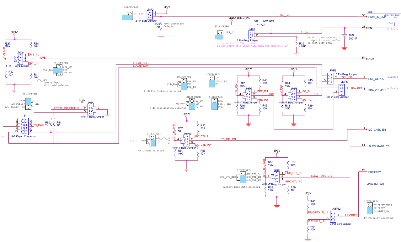 Figure 30. Configuration Options
9.2.2.3 Dual Layout for Single or Dual Power Supply
The SN75DP126DS requires dual power supply whereas the DP126SS requires only one power supply. The design can have options to use either one with minor hardware changes
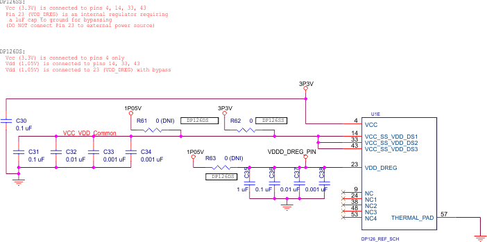 Figure 31. Power Supply Layout
9.2.3 Application Curves
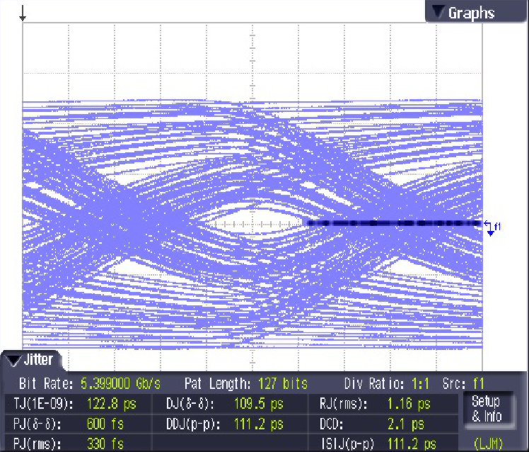
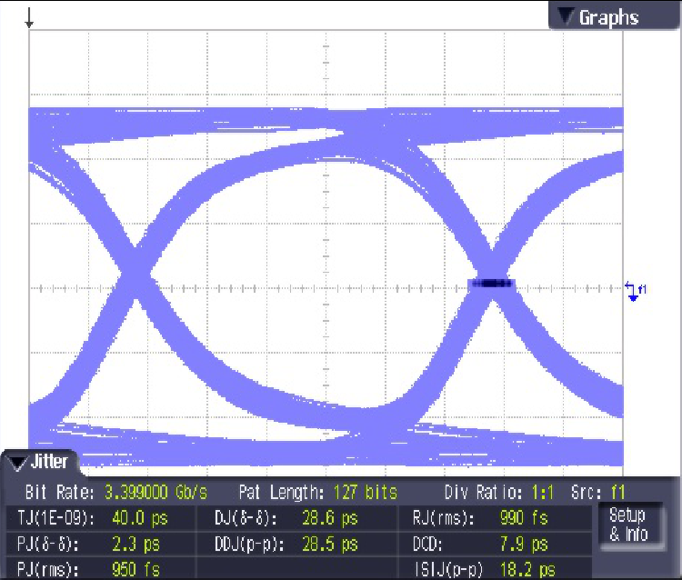
DisplayPort Sink
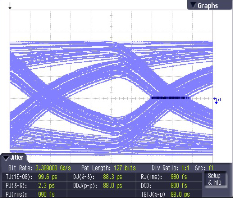
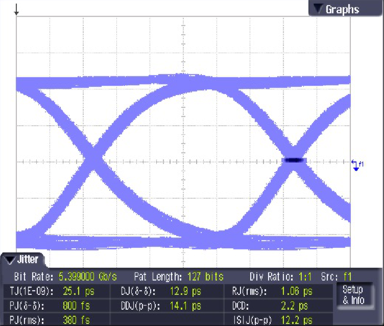
15 dB EQ Setting; DP Sink
