SLLSE57E April 2011 – March 2015 SN75DP130
PRODUCTION DATA.
- 1 Features
- 2 Applications
- 3 Description
- 4 Revision History
- 5 Description (continued)
- 6 Pin Configuration and Functions
- 7 Specifications
- 8 Parameter Measurement Information
- 9 Detailed Description
- 10Application and Implementation
- 11Power Supply Recommendations
- 12Layout
- 13Device and Documentation Support
- 14Mechanical, Packaging, and Orderable Information
Package Options
Mechanical Data (Package|Pins)
- RGZ|48
Thermal pad, mechanical data (Package|Pins)
- RGZ|48
Orderable Information
10 Application and Implementation
NOTE
Information in the following applications sections is not part of the TI component specification, and TI does not warrant its accuracy or completeness. TI’s customers are responsible for determining suitability of components for their purposes. Customers should validate and test their design implementation to confirm system functionality.
10.1 Application Information
The SN75DP130 offers separate AUX and DDC source interfaces that connect to a single AUX sink channel. This minimizes component count when implemented with a graphics processor (GPU) comprising separate DDC and AUX interfaces. For GPUs with combined DDC/AUX, the device can operate as a FET switch to short circuit the AUX channel AC coupling caps while connected to a TMDS sink device.
The configuration shown in Figure 21 supports a GPU with separate DDC and AUX interfaces, and overcomes the need for an external AUX to DDC switch. This circuit provides back current protection into the GPU AUX, HPD, and CAD inputs.
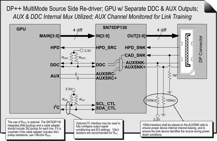 Figure 21. DP++ Dual-Mode in a Split AUX/DDC Configuration
The configuration shown in Figure 22 is preferred to avoid very long AUX signal stub lines. Furthermore, this configuration provides isolation between the DP connector and the GPU.
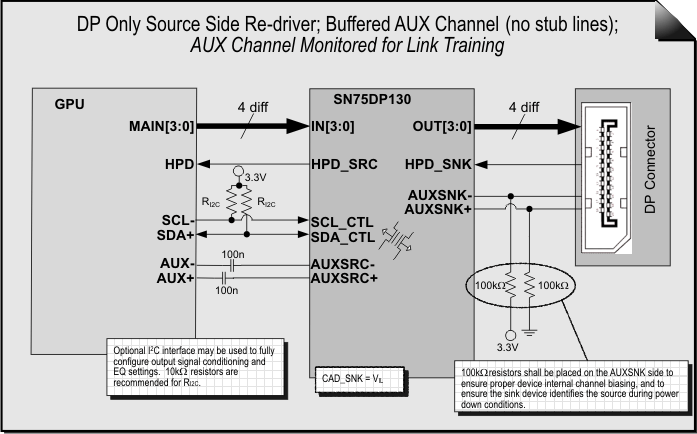 Figure 22. DP Only Configuration with AUX Pass Through
The configuration shown in Figure 23 enables the SN75DP130 in DP++ Dual-Mode with the AUX input only monitoring the AUX channel. Use this setting when AUX stub lines can be kept short and minimum AUX attenuation is desired. For DP v1.1a, the stub length shall not exceed 4cm each, and for DP v1.2 with FAUX support each stub line shall be shorter than 1cm.
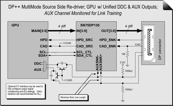 Figure 23. DP++ Dual-Mode Configuration with AUX Monitor
The alternate configuration shown in Figure 24 allows a reduced BOM by eliminating the need for external FET switches while routing AUX and DDC externally, which eliminates any insertion loss cases of AUX is brought through the SN75DP130. For DP v1.2 with FAUX support each stub line shall be shorter than 1cm.
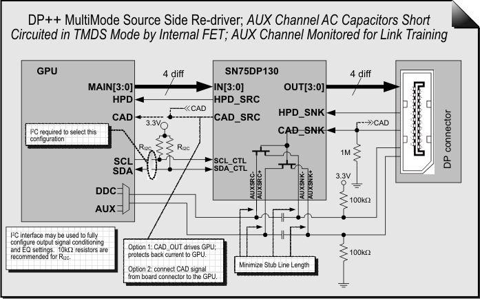 Figure 24. Alternate Low-BOM DP++ Dual-Mode Configuration
The previous application examples were specifically concerned with source side implementations of the SN75DP130. Even though source applications (notebook, docking station, and so forth) are the primary target application for the DP130A, the DP130A can also be used in a sink application, such as a DisplayPort monitor. The reader is referred to SLLA349 (Implementation Guide: DP130 in a Sink) for a detailed discussions of the implementation guidelines for sink applications.
10.2 Typical Application
The configuration shown in Figure 25 supports a GPU with unified AUX/DDC interfaces. This circuit provides back current protection into the GPU AUX, HPD, and CAD inputs.
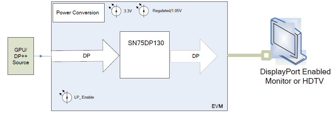 Figure 25. Typical Application Schematic
10.2.1 Design Requirements
For this design example, use the parameters listed in Table 30 as the input parameters.
Table 30. Design Parameters
| DESIGN PARAMETERS | VALUE |
|---|---|
| VCC power supply | 3.3 V |
| VDD power supply | 1.1 V |
| DP single-ended impedance | 50 Ω |
10.2.2 Detailed Design Procedure
10.2.2.1 Logic I2C Interface
The internal registers of the SN75DP130 are accessed through the SCL_CTL pin and 3 SDA_CTL pin. The 7-bit I2C slave address of the DP130 is determined by the ADDR_EQ pin 4.
Table 31. I2C Slave Address Selection
| ADDR_EQ | 7-BIT I2C SLAVE ADDRESS | READ SLAVE ADDRESS | WRITE SLAVE ADDRESS |
|---|---|---|---|
| Low (VIL) | 7’b0101100 | 'h59 | 'h58 |
| VCC/2 (VIM) | 7’b0101101 | 'h5B | 'h5A |
| High (VIH) | 7’b0101110 | 'h5D | 'h5C |
10.2.2.2 CAD Sink Over Ride
For testing and debug purposes, leave a place holder on the CAD_SNK input in order to have the option to independently set the DP130 in DP or TMDS mode. A 2k pull-up on this place holder will set the DP130 in TMDS mode independent of the Sink.
10.2.2.3 HPD Sink Over Ride
For testing and debug purposes, leave a place holder on the HPD_SNK input in order to have the option to force the presence of the sink. A 2k pull-up on this place holder will provide an indication of the sink presence.
10.2.3 Application Curves
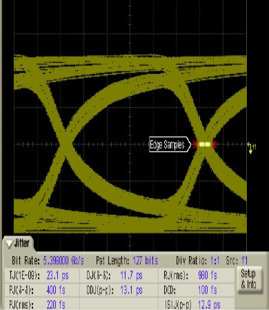 Figure 26. Input Into DP130
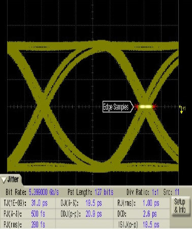 Figure 27. Eye Diagram (EQ = 3.5 dB)
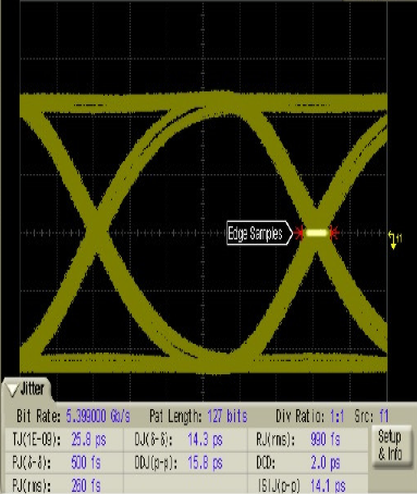 Figure 28. Eye Diagram (EQ = 6 dB)
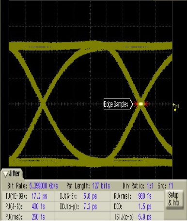 Figure 30. Eye Diagram (EQ = 10 dB)
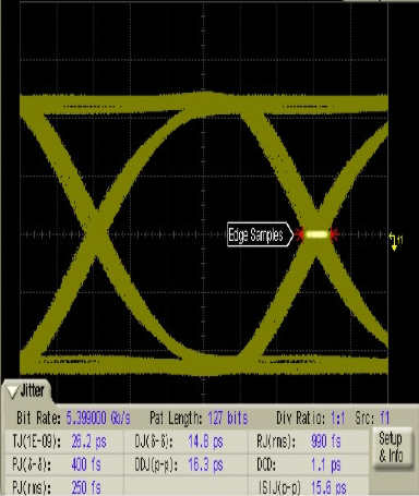 Figure 32. Eye Diagram (EQ = 15 dB)
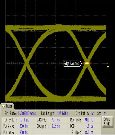 Figure 29. Eye Diagram (EQ = 8 dB)
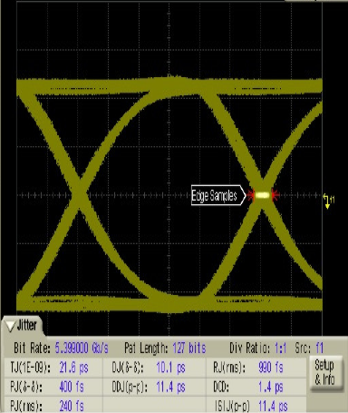 Figure 31. Eye Diagram (EQ = 13 dB)
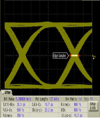 Figure 33. Eye Diagram (EQ = 18 dB)