SBFS022C June 2003 – October 2015 SRC4192 , SRC4193
PRODUCTION DATA.
- 1 Features
- 2 Applications
- 3 Description
- 4 Revision History
- 5 Pin Configuration and Functions
- 6 Specifications
- 7 Detailed Description
- 8 Application and Implementation
- 9 Power Supply Recommendations
- 10Layout
- 11Device and Documentation Support
- 12Mechanical, Packaging, and Orderable Information
Package Options
Refer to the PDF data sheet for device specific package drawings
Mechanical Data (Package|Pins)
- DB|28
Thermal pad, mechanical data (Package|Pins)
Orderable Information
7 Detailed Description
7.1 Overview
The SRC4192 and SRC4193 devices are asynchronous, sample-rate converters (ASRC) designed for professional audio applications. Operation at input and output sampling frequencies up to 212 kHz is supported, with an input and output sampling ratio range of 16:1 to 1:16. Excellent dynamic range and Total Harmonic Distortion + Noise (THD+N) are achieved by employing high-performance, linear-phase digital filtering with image rejection better than 140 dB. Digital filtering options allow for lower group-delay processing. These include a low group-delay option for the interpolation and resampler function, as well as a direct down-sampling option for the decimation function (SRC4193 device only).
The audio input and output ports support standard audio data formats, as well as a TDM interface mode. Word lengths of 24-, 20-, 18-, and 16-bits are supported. Both ports may operate in slave mode, deriving their word and bit clocks from external input and output devices. Alternatively, one port may operate in master mode while the other remains in slave mode. In master mode, the LRCK and BCK clocks are derived from the reference clock input, RCKI. The flexible configuration of the input and output ports allows connection to a wide variety of audio data converters, interface devices, digital signal processors, and programmable logic.
A bypass mode is included, which allows audio data to be passed directly from the input port to the output port, bypassing the ASRC function. The bypass option is useful for passing through encoded or compressed audio data, or nonaudio control or status data.
A soft mute function is available on both the SRC4192 and SRC4193 devices. Digital output attenuation is available only for the SRC4193 device. Both soft mute and digital attenuation functions provide artifact-free operation, while allowing muting or level adjustment of the audio output signal. The mute attenuation is typically –144 dB, while the digital attenuation control is adjustable from 0 dB to –127.5 dB in 0.5-dB steps.
The SRC4193 device includes a three-wire SPI port to access on-chip control registers for configuration of internal functions. The port can be easily interfaced to microprocessors or digital signal processors with synchronous serial port peripherals.
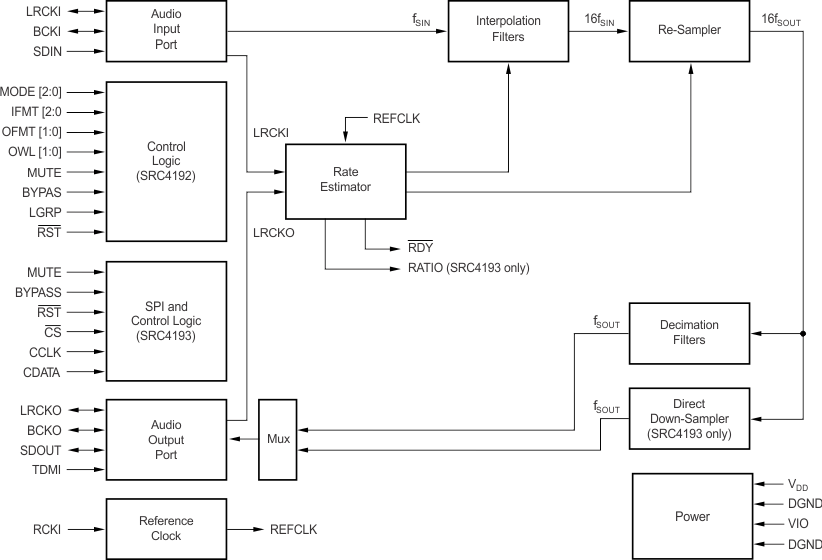
Functional Block Diagram shows a functional block diagram of the SRC4192 and SRC4193 devices. Audio data is received at the input port, clocked by either the audio data source in slave mode, or by the SRC419x in master mode. The output-port data is clocked by either the audio data source in slave mode, or by the SRC419x in master mode. The input data is passed through interpolation filters which up-sample the data, which is then passed on to the resampler. The rate estimator compares the input and output sampling frequencies by comparing LRCKI, LRCKO, and a reference clock. The results include an offset for the FIFO pointer and the coefficients needed for re-sampling function.
The output of the resampler is passed on to either the decimation filter or direct down-sampler function. The decimation filter performs down-sampling and anti-alias filtering functions, and is required when the output sampling frequency is lower than the input-sampling frequency. The direct down-sampler function does not provide any filtering, and may be used in cases when aliasing is not an issue. This includes the case when the output sampling frequency is equal to or greater than the input sampling frequency. The advantage of direct down-sampling is a significant reduction in the group delay associated with the decimation filter, allowing lower latency sample rate conversion. The direct down-sampler function is available only for the SRC4193 device.
7.2 Functional Block Diagram
7.3 Feature Description
7.3.1 Input Port Operation
The audio input port is a three-wire synchronous serial interface that can operate in either slave or master mode. The SDIN input (pin 4) is the serial audio data input. Audio data is input at this pin in one of three standard audio data formats: Philips I2S, Left-Justified, or Right-Justified. The audio data word length may be up to 24-bits for I2S and Left-Justified formats, while the Right-Justified format supports 16-, 18-, 20-, or 24-bit data. The data formats are shown in Figure 59, while critical timing parameters are shown in Figure 60 and listed in Electrical Characteristics.
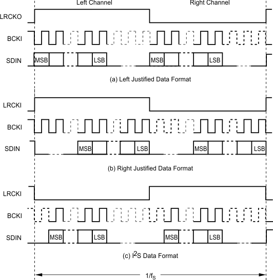 Figure 59. Input Data Formats
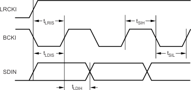 Figure 60. Input Port Timing
The bit clock is either an input or output at BCKI (pin 5). In slave mode, BCKI is configured as an input pin, and may operate at rates from 32fS to 128fS,with a minimum of one clock cycle per data bit. In master mode, BCKI operates at a fixed rate of 64fS.
The left/right word clock, LRCKI (pin 6), may be configured as an input or output pin. In slave mode, LRCKI is an input pin, while in master mode LRCKI is an output pin. In either case, the clock rate is equal to fS, the input sampling frequency. The LRCKI duty cycle is fixed to 50% for master mode operation.
Table 1 shows data format selection for the input port. For the SRC4192, the IFMT0 (pin 10), IFMT1 (pin 11), and IFMT2 (pin 12) inputs are used to set the input port data format. For the SRC4193, the IFMT[2:0] bits in Control Register 3 are used to select the data format.
Table 1. Input Port Data Format Selection
| IFMT2 | IFMT1 | IFMT0 | INPUT PORT DATA FORMAT |
|---|---|---|---|
| 0 | 0 | 0 | 24-Bit Left Justified |
| 0 | 0 | 1 | 24-Bit I2S |
| 0 | 1 | 0 | Unused |
| 0 | 1 | 1 | Unused |
| 1 | 0 | 0 | 16-Bit Right Justified |
| 1 | 0 | 1 | 18-Bit Right Justified |
| 1 | 1 | 0 | 20-Bit Right Justified |
| 1 | 1 | 1 | 24-Bit Right Justified |
7.3.2 Output Port Operation
The audio output port is a four-wire synchronous serial interface that can operate in either Slave or Master mode. The SDOUT output (pin 23) is the serial audio data output. Audio data is output at this pin in one of four data formats: Philips I2S, Left-Justified, Right-Justified, or TDM. The audio data word length may be 16-, 18-, 20-, or 24-bits. For all word lengths, the data is triangular PDF dithered from the internal 28-bit data path. The data formats (with the exception of TDM mode) are shown in Figure 61, while critical timing parameters are shown in Figure 62 and listed in Electrical Characteristics. The TDM format and timing are shown in Figure 72 and Figure 73, respectively, while examples of standard TDM configurations are shown in Figure 74 and Figure 75
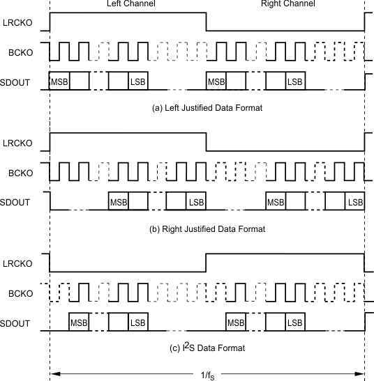 Figure 61. Output Data Formats
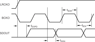 Figure 62. Output Port Timing
The bit clock is either input or output at BCKO (pin 25). In Slave mode, BCKO is configured as an input pin, and can operate at rates from 32fS to 128fS, with a minimum of one clock cycle for each data bit. The exception is the TDM mode, where the BCKO must operate at N × 64fS, where N is equal to the number of SRC4192 or SRC4193 devices included on the TDM interface. In master mode, BCKO operates at a fixed rate of 64fS for all data formats except TDM, where BCKO operates at the reference clock (RCKI) frequency. Additional information regarding TDM mode operation is included in Application and Implementation.
The left/right word clock, LRCKO (pin 24), can be configured as an input or output pin. In slave mode, LRCKO is an input pin, while in master mode it is an output pin. In either case, the clock rate is equal to fS, the output sampling frequency. The clock duty cycle is fixed to 50% for I2S, Left-Justified, and Right-Justified formats in master mode. The LRCKO pulse width is fixed to 32 BCKO cycles for the TDM format in master mode.
Table 2 illustrates data format selection for the output port. For the SRC4192, the OFMT0 (pin 19), OFMT1 (pin 18), OWL0 (pin 17), and OWL1 (pin 16) inputs are used to set the output port data format and word length. For the SRC4193, the OFMT[1:0] and OWL[1:0] bits in Control Register 3 are used to select the data format and word length.
Table 2. Output Port Data Format Selection
| OFMT1 | OFMT0 | OUTPUT PORT DATA FORMAT |
|---|---|---|
| 0 | 0 | Left-Justified |
| 0 | 1 | I2S |
| 1 | 0 | TDM |
| 1 | 1 | Right-Justified |
| OWL1 | OWL0 | OUTPUT PORT DATA WORD LENGTH |
| 0 | 0 | 24-Bits |
| 0 | 1 | 20-Bits |
| 1 | 0 | 18-Bits |
| 1 | 1 | 16-Bits |
7.3.3 Soft Mute Function
The soft mute function of the SRC419x device is invoked by forcing the MUTE input (pin 14) high. For the SRC4193 device, the mute function may also be accessed using the MUTE bit in Control Register 1. The soft mute function slowly attenuates the output signal level down to all zeroes plus ±1LSB of dither. This provides an artifact-free muting of the audio output port.
7.3.4 Digital Attenuation (SRC4193 Only)
The SRC4193 device includes independent digital attenuation for the left and right audio channels. The attenuation ranges from 0 dB (or unity) to –127.5 dB in 0.5-dB steps. The attenuation settings are programmed using Control Registers 4 and 5, corresponding to the left and right channels, respectively.
The TRACK bit in Control Register 1 selects independent or tracking attenuation modes. When TRACK = 0, the left and right channels are controlled independently. When TRACK = 1, the attenuation setting for the left channel is also used for the right channel, and the right channel is said to track the left channel attenuation setting.
7.3.5 Ready Output
The SRC419x device includes an active low ready output named RDY (pin 15). This is an output from the rate estimator block, which indicates that the input-to-output sampling frequency ratio has been determined. The ready signal can be used as a flag or indicator output. The ready signal can also be connected to the active high MUTE input (pin 14) to provide an auto-mute function, so that the output port is muted when the rate estimator is in transition.
7.3.6 Ratio Output (SRC4193 Only)
The SRC4193 device includes a simple ratio flag output named RATIO (pin 16). When RATIO is low, it indicates that the output sampling frequency is lower than the input sampling frequency. When RATIO is high, it indicates that the output sampling frequency is higher than the input sampling frequency. The ratio output can be used as an indicator or flag output for an LED or host device.
7.3.7 Serial Peripheral Interface (SPI) Port: SRC4193 Only
The SPI port is a three-wire synchronous serial interface used to access the on-chip control registers of the SRC4193 device. The interface is comprised of a serial data clock input, CCLK (pin 27), a serial data input, CDATA (pin 28), and an active low chip-select input, CS (pin 26). Figure 63 shows the protocol for writing control registers using the serial control port. Figure 64 shows the critical timing parameters for the SPI port interface, which are also listed in Electrical Characteristics.
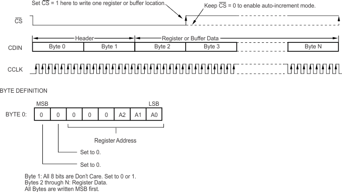 Figure 63. SPI Port Protocol
 Figure 64. SPI Port Timing
Byte 0 indicates the address of the control register to be written. The two most significant bits are set to 0, while the six least significant bits contain the control register address. Byte 1 is a don’t care byte. This byte is included in the protocol to maintain compatibility with current and future Texas Instruments digital audio products, including the DIT4096 and DIT4192 digital audio transmitters. Byte 2 contains the 8-bit data for the control register addressed in Byte 0.
As shown in Figure 63, a write sequence starts by bringing the CS input low. Bytes 0, 1, and 2 are then written to program a single control register. Bringing the CS input high after the third byte will write just one register. However, if CS remains low after writing the first control byte, the port will autoincrement the address by 1, allowing successive addresses to be written. The address is automatically incremented by 1 after each byte is written, as long as the CS input remains low. This is referred to as auto-increment operation, and is always enabled for the SPI port.
7.4 Device Functional Modes
7.4.1 Reset and Power Down Operation
The SRC419x device can be reset using the RST input (pin 13). There is no internal power-on reset, so the user should force a reset sequence after power up to initialize the device. To force a reset, the reference clock input must be active, with an external clock source supplying a valid reference clock signal (refer to Figure 80). The user must assert RST low for a minimum of 500 ns, and then bring RST high again to force a reset. Figure 65 shows the reset timing for the SRC419x device.
For the SRC4193, there is an additional 500 µs delay after the RST rising edge, due to internal logic requirements. The customer should wait at least 500 µs after the RST rising edge before attempting to write to the SPI port of the SRC4193 device.
The SRC419x device also supports a power-down mode. Power-down mode may be set by either holding the RST input low (SRC4192 and SRC4193 devices), or by setting the PDN bit in Control Register 1 to zero (SRC4193 device only). The SRC4193 device will be in power-down mode by default after an external reset has been issued. To enable normal operation for the SRC4193, disable power down mode by writing a 1 to the PDN bit in Control Register 1.
When using the PDN bit in Control Register 1 to enable power-down mode for the SRC4193, the current state of the control registers is maintained through the power-down and power-up transition.
 Figure 65. Reset Pulse Width Requirement
7.4.2 Audio Port Modes
The SRC4192 and SRC4193 devices both support seven serial-port modes, shown in Table 3. For the SRC4192 device, the audio port mode is selected using the MODE0 (pin 26), MODE1 (pin 27), and MODE2 (pin 28) inputs. For the SRC4193 device, the mode is selected using the MODE[2:0] bits in Control Register 1. The default mode setting for the SRC4193 device is both input and output ports set to slave mode.
In slave mode, the port LRCK and BCK clocks are configured as inputs, and receive their clocks from an external audio device. In master mode, the LRCK and BCK clocks are configured as outputs, being derived from the reference clock input (RCKI). Only one port can be set to master mode at any given time, as indicated in Table 3.
Table 3. Setting the Serial Port Modes
| MODE2 | MODE1 | MODE0 | SERIAL PORT MODE |
|---|---|---|---|
| 0 | 0 | 0 | Both Input and Output Ports are Slave mode |
| 0 | 0 | 1 | Output Port is Master mode with RCKI = 128 fS |
| 0 | 1 | 0 | Output Port is Master mode with RCKI = 512 fS |
| 0 | 1 | 1 | Output Port is Master mode with RCKI = 256 fS |
| 1 | 0 | 0 | Both Input and Output Ports are Slave mode |
| 1 | 0 | 1 | Input Port is Master mode with RCKI = 128 fS |
| 1 | 1 | 0 | Input Port is Master mode with RCKI = 512 fS |
| 1 | 1 | 1 | Input Port is Master mode with RCKI = 256 fS |
7.4.3 Bypass Mode
The SRC419x device includes a bypass function, which routes the input port data directly to the output port bypassing the ASRC function. Bypass mode may be invoked by forcing the BYPAS input (pin 9) high for the devices. The bypass mode may also be accessed for the SRC4193 device using the BYPAS bit in Control Register 1. The BYPAS pin and control bit should be set to 0 for normal operation.
No dithering is applied to the output data in bypass mode, and the digital attenuation and mute functions are also unavailable.
7.5 Register Maps
Control Register Map (SRC4193 Device Only)
The control register map for the SRC4193 device is shown in Table 4. Register 0 is reserved for factory use and defaults to all zeros upon reset. Avoid writing this register, as unexpected operation may result if Register 0 is programmed to an arbitrary value. Registers 1 through 5 contain control bits used to configure the internal functions of the SRC4193. All other register addresses are reserved and should not be used in customer applications.
Table 4. SRC4193 Device Control Register Map
| Register Address (Dec/Hex) |
D7 (MSB) | D6 | D5 | D4 | D3 | D2 | D1 | D0 (LSB) |
|---|---|---|---|---|---|---|---|---|
| 0 | 0 | 0 | 0 | 0 | 0 | 0 | 0 | 0 |
| 1 | PDN | TRACK | 0 | MUTE | BYPAS | MODE2 | MODE1 | MODE0 |
| 2 | 0 | 0 | 0 | 0 | 0 | 0 | DFLT | LGRP |
| 3 | OWL1 | OWL0 | OFMT1 | OFMT0 | 0 | IFMT2 | IFMT1 | IFMT0 |
| 4 | AL7 | AL6 | AL5 | AL4 | AL3 | AL2 | AL1 | AL0 |
| 5 | AR7 | AR6 | AR5 | AR4 | AR3 | AR2 | AR1 | AR0 |
7.5.0.1 System Control Register
Table 5. System Control Register Field Descriptions
| Bit | Field | Description |
|---|---|---|
| 7 | PDN |
Power Down Setting this bit to 0 sets the SRC4193 to the power-down state. All other register settings are preserved and the SPI port remains active. (Default) Setting this bit to 1 powers up the SRC4193 using the current register settings. |
| 6 | TRACK |
Digital Attenuation Tracking 0 = Tracking Off: Attenuation for the Left and Right channels is controlled independently. (Default) 1 = Tracking On: Left channel attenuation setting is used for both channels. |
| 5 | Reserved | |
| 4 | MUTE |
Output Soft Mute This bit is logically OR’d with the MUTE input (pin 14) 0 = Soft mute disabled (Default) 1 = Soft mute enabled with data attenuated to all 0s |
| 3 | BYPAS |
Bypass Mode This bit is logically OR’d with the BYPAS input (pin 9) 0 = Bypass Mode disabled with normal ASRC operation. (Default) 1 = Bypass Mode enabled with data routed directly from the input port to the output port, bypassing the ARSC function. |
| 2-0 | MODEx |
Audio Serial Port Mode See Table 3. |
7.5.0.2 Filter Control Register
| 7 | 6 | 5 | 4 | 3 | 2 | 1 | 0 |
| Reserved | DFLT | LGRP | |||||
| LEGEND: R/W = Read/Write; R = Read only; -n = value after reset |
Table 6. Filter Control Register Field Descriptions
| Bit | Field | Description |
|---|---|---|
| 7-2 | Reserved | |
| 1 | DFLT |
Decimation Filtering / Direct Down-Sampling The DFLT bit enables or disables the direct down-sampling function. 0 = Decimation filter enabled (default) (Must be used when fSOUT is less than fSIN) 1 = Direct down-sampling enabled without filtering. (May be enabled when fSOUT is equal to or greater than fSIN) |
| 0 | LGRP |
Low Group Delay This bit selects the number of input audio samples to be stored in the data buffer before the ASRC starts processing the audio data. 0 = Normal delay, 64 samples (default) 1 = Low delay, 32 samples |
7.5.0.3 Audio Data Format Register
| 7 | 6 | 5 | 4 | 3 | 2 | 1 | 0 |
| OWL1 | OWL0 | OFMT1 | OFMT0 | Reserved | IFMT2 | IFMT1 | IFMT0 |
| LEGEND: R/W = Read/Write; R = Read only; -n = value after reset |
7.5.0.4 Digital Attenuation Register – Left Channel
| 7 | 6 | 5 | 4 | 3 | 2 | 1 | 0 |
| AL7 | AL6 | AL5 | AL4 | AL3 | AL2 | AL1 | AL0 |
| LEGEND: R/W = Read/Write; R = Read only; -n = value after reset |
Table 8. Digital Attenuation Register – Left Channel Field Descriptions
| Bit | Field | Description |
|---|---|---|
| 7-0 | ALx |
Register defaults to 00HEX, or 0 dB (unity gain). Output Attenuation (dB) = (–N × 0.5), where N = AL[7:0]DEC |
7.5.0.5 Digital Attenuation Register – Right Channel
| 7 | 6 | 5 | 4 | 3 | 2 | 1 | 0 |
| AR7 | AR6 | AR5 | AR4 | AR3 | AR2 | AR1 | AR0 |
| LEGEND: R/W = Read/Write; R = Read only; -n = value after reset |
Table 9. Digital Attenuation Register – Right Channel Field Descriptions
| Bit | Field | Description |
|---|---|---|
| 7-0 | ARx |
Register defaults to 00HEX, or 0 dB (unity gain). Output Attenuation (dB) = (–N × 0.5), where N = AR[7:0]DEC When the TRACK bit in Control Register 1 is set to 1, the Left Channel attenuation setting will be used for the Right Channel attenuation. |