SBFS022C June 2003 – October 2015 SRC4192 , SRC4193
PRODUCTION DATA.
- 1 Features
- 2 Applications
- 3 Description
- 4 Revision History
- 5 Pin Configuration and Functions
- 6 Specifications
- 7 Detailed Description
- 8 Application and Implementation
- 9 Power Supply Recommendations
- 10Layout
- 11Device and Documentation Support
- 12Mechanical, Packaging, and Orderable Information
Package Options
Refer to the PDF data sheet for device specific package drawings
Mechanical Data (Package|Pins)
- DB|28
Thermal pad, mechanical data (Package|Pins)
Orderable Information
10 Layout
10.1 Layout Guidelines
10.1.1 Reference Clock
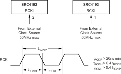
The SRC4192 and SRC4193 devices require a reference clock for operation. The reference clock is applied at the RCKI input (pin 1 for the SRC4193 device, pin 2 for the SRC4192 device). Figure 80 shows the reference clock connections and requirements for the SRC4192 and SRC4193 devices. The reference clock may operate at 128fS, 256fS, or 512fS, where fS are the input or output sampling frequency. The maximum external reference clock input frequency is 50 MHz.
 Figure 80. Reference Clock Input Connections and Timing Requirements
10.1.2 Pin Compatibility With the Analog Devices AD1896 (SRC4192 Only)
The SRC4192 device is pin-and function-compatible with the AD1896 device when observing the guidelines indicated in the following paragraphs.
10.1.2.1 Crystal Oscillator
The SRC4192 does not have an on-chip crystal oscillator. An external reference clock is required at the RCKI input (pin 2).
10.1.2.2 Reference Clock Frequency
The reference clock input frequency for the SRC4192 must be no higher than 30 MHz, to match the master clock frequency specification of the AD1896 device. In addition, the SRC4192 device does not support the 768fS reference clock rate.
10.1.2.3 Master Mode Maximum Sampling Frequency
When the input or output ports are set to master mode, the maximum sampling frequency must be limited to 96 kHz to support the AD1896 device specification. This is despite the fact that the SRC4192 device supports a maximum sampling frequency of 212 kHz in master mode. The user should consider building an option into their design to support the higher sampling frequency of the SRC4192 device.
10.1.2.4 Matched Phase Mode
Because of the internal architecture of the SRC4192 device, it does not require or support the matched phase mode of the AD1896 device. Given multiple SRC4192 devices, if all reference clock (RCKI) inputs are driven from the same clock source, the devices will be phase-matched.
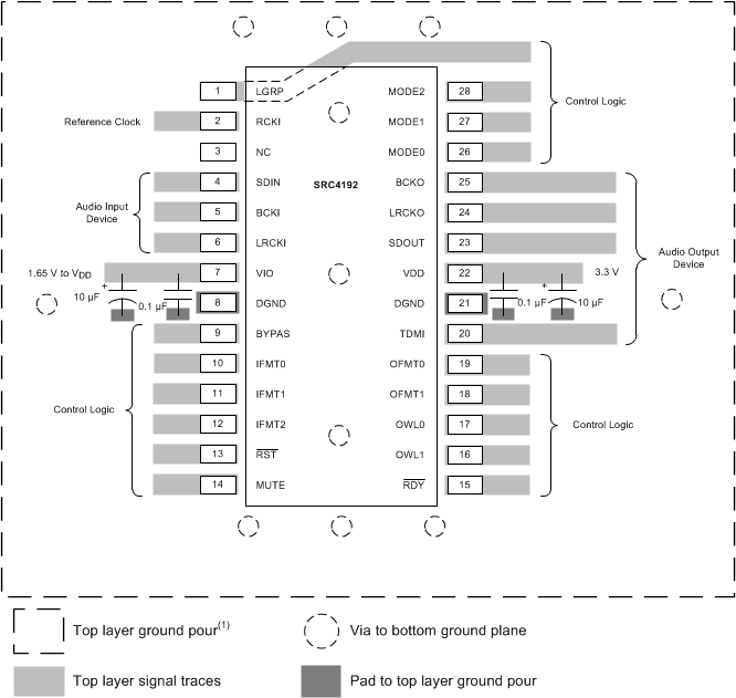
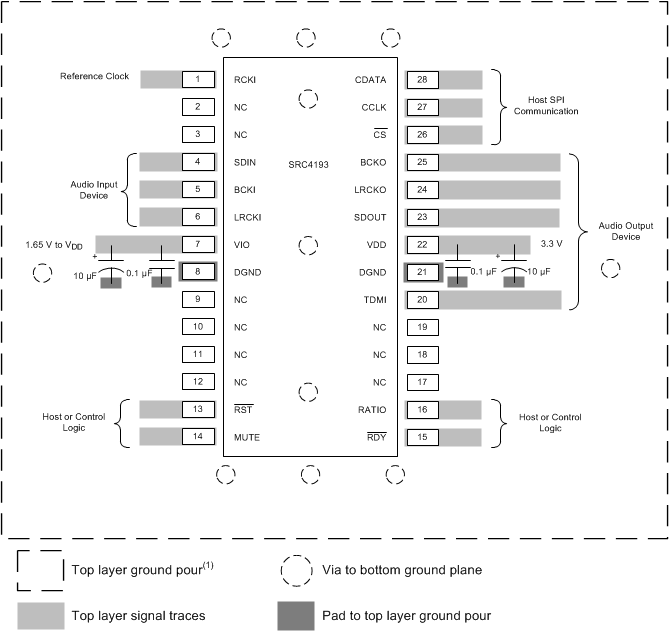
10.2 Layout Example

